

Search results
Search for "charge compensation" in Full Text gives 32 result(s) in Beilstein Journal of Nanotechnology.
Imaging of carbon nanomembranes with helium ion microscopy
Beilstein J. Nanotechnol. 2015, 6, 1712–1720, doi:10.3762/bjnano.6.175

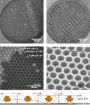
- can visualize them. However, CNMs are electrically insulating, which makes them sensitive to charging. We demonstrate that the helium ion microscope (HIM) is a good candidate for imaging freestanding CNMs due to its efficient charge compensation tool. Scanning with a beam of helium ions while
- report, we will show examples that support this statement. We demonstrate the effect of charging on HIM images as well as the effectiveness of the HIM charge compensation mechanism. The principle of operation of HIM as well as a recent overview of HIM-related reports can be found elsewhere [17]. In short
- well as charge compensation can reduce or completely avoid the charging of insulating membranes. These imaging parameter changes resulted in Figure 1d, which does not show any notable charging effects. Here, the sample was mounted in a way that no secondary electrons from the sample holder could reach




Scanning reflection ion microscopy in a helium ion microscope
Beilstein J. Nanotechnol. 2015, 6, 1125–1137, doi:10.3762/bjnano.6.114

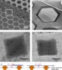
- detectable step height was found to be approximately 5 nm. RIM imaging of an insulator surface without the need for charge compensation was successfully demonstrated. Keywords: helium ion microscope; low-angle ion scattering; reflection microscopy; surface imaging; surface morphology; Introduction
- microscopy of cleaved mica Figure 6 shows an RI image of a cleaved mica surface obtained at a magnification of 100,000× under the grazing angle of 5° without charge compensation or conductive coatings. One can see that all details of the step-like surface are well reproduced without any noticeable image
- incidence from 0° to 10° results in the relative variation of the shadow width of a few percent and does not affect the accuracy of the measurements. In summary, reflection ion microscopy is useful for imaging of the surface of dielectric materials without the need for charge compensation, and the


Towards bottom-up nanopatterning of Prussian blue analogues
Beilstein J. Nanotechnol. 2014, 5, 1933–1943, doi:10.3762/bjnano.5.204
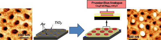
- were collected at a pass energy of 10 eV for S 2p core XPS levels. No charge compensation was applied during acquisition. Results and Discussion The gold layer The silicon wafer and the samples Au10, Au20 and Au50 were studied by AFM. Representative AFM images are shown in Figure 1. After gold


Near-field photochemical and radiation-induced chemical fabrication of nanopatterns of a self-assembled silane monolayer
Beilstein J. Nanotechnol. 2014, 5, 1441–1449, doi:10.3762/bjnano.5.156

- (Figure 4c). This indicates that in this case a double layer of the negatively charged gold nanoparticles might be adsorbed. Unlike in the case of the specific chemical binding of the fluorescein tags, more or less than a monolayer can be bound to the positively charged nanopattern due to charge
- compensation, depending on the surface charges of the nanopattern and of the nanoparticles which may alter their properties under different conditions of the sample preparation. For the 0.22 µm nanopattern, which cannot be identified in the fluorescence images, the topography images taken on the same


Towards precise defect control in layered oxide structures by using oxide molecular beam epitaxy
Beilstein J. Nanotechnol. 2014, 5, 596–602, doi:10.3762/bjnano.5.70

- , for instance, to solubility limits or to the tendency of atoms intermixing at interfaces resulting in cationic redistribution or intergrowth of secondary phases. Moreover, how do charge compensation mechanisms act at interfaces? What is the result of the “polar discontinuity” and of the presence of


Site-selective growth of surface-anchored metal-organic frameworks on self-assembled monolayer patterns prepared by AFM nanografting
Beilstein J. Nanotechnol. 2013, 4, 638–648, doi:10.3762/bjnano.4.71
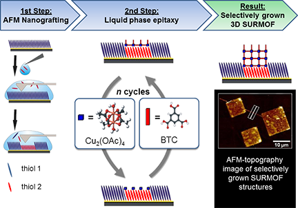
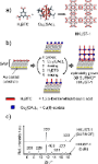
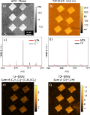
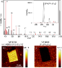
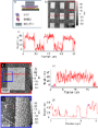
- about 200 nm with nominal mass resolution (burst alignment mode). No charge compensation was required. Spectra were calibrated on omnipresent C−, CH−, CH2−, Au−, and molecular peaks. (a) Building units for the growth of MOF HKUST-1 and the unit cell of HKUST-1. (b) The principle of the layer-by-layer





Noncontact atomic force microscopy study of the spinel MgAl2O4(111) surface
Beilstein J. Nanotechnol. 2012, 3, 192–197, doi:10.3762/bjnano.3.21

- Co3O4(111) films with the spinel structure [13][14] show evidence for an apparently unreconstructed (1×1) surface, the stability of which was proposed to be based on a Co2+/Co3+ inversion process leading to charge compensation. In the present case of MgAl2O4(111), no previous experimental studies are


Other Beilstein-Institut Open Science Activities