

Search results
Search for "electron beam evaporation" in Full Text gives 52 result(s) in Beilstein Journal of Nanotechnology.
Generation and agglomeration behaviour of size-selected sub-nm iron clusters as catalysts for the growth of carbon nanotubes
Beilstein J. Nanotechnol. 2011, 2, 734–739, doi:10.3762/bjnano.2.80
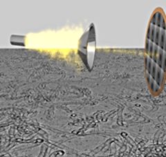
- either thermal evaporation (heating Al in a boron nitride crucible with a tungsten filament) or electron beam evaporation onto a commercial TEM grid (SiOx; Fa. Plano, Wetzlar). Aluminium buffer layer (10 nm) deposition was monitored by means of a quartz crystal microbalance (Cressington MTM 10). After


Formation of precise 2D Au particle arrays via thermally induced dewetting on pre-patterned substrates
Beilstein J. Nanotechnol. 2011, 2, 318–326, doi:10.3762/bjnano.2.37

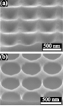
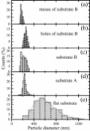
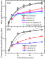
- with thicknesses of 10 nm, 20 nm, 40 nm and 60 nm on the pre-patterned substrates using electron beam evaporation at a base pressure of 2 × 10⁻⁷ mbar. Film thicknesses were determined by the quartz crystal monitor and then verified by profilometer measurements (Dektak 150 – Veeco). After deposition





Other Beilstein-Institut Open Science Activities