

Search results
Search for "magnetron sputtering" in Full Text gives 132 result(s) in Beilstein Journal of Nanotechnology.
A highly pH-sensitive nanowire field-effect transistor based on silicon on insulator
Beilstein J. Nanotechnol. 2013, 4, 330–335, doi:10.3762/bjnano.4.38

- and contact pads. Aluminium mask e-beam vapour deposition. Anisotropic reactive ion etching of the device layer through the Al mask and mask removal. Magnetron sputtering of titanium electrodes and their isolation with silica to allow measurements in liquids. Both optical and electron-beam lithography


Hydrogen-plasma-induced magnetocrystalline anisotropy ordering in self-assembled magnetic nanoparticle monolayers
Beilstein J. Nanotechnol. 2013, 4, 164–172, doi:10.3762/bjnano.4.16

- gradient magnetometer (AGM) measurements were performed before and after plasma treatment. Since a significant degree of oxidation can occur on very short time scales [15][16], the samples were covered in situ with a thin protective layer. These layers were deposited employing magnetron sputtering. For


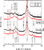


Sub-10 nm colloidal lithography for circuit-integrated spin-photo-electronic devices
Beilstein J. Nanotechnol. 2012, 3, 884–892, doi:10.3762/bjnano.3.98

- SiO2, we etch two times longer (2 min) in order to form a good undercut in SiO2, which is important for the following deposition steps. Magnetron sputtering was used for deposition of the active point-contact region. The material combination was selected to represent the spin-injection laser device [15
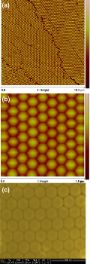


Highly ordered ultralong magnetic nanowires wrapped in stacked graphene layers
Beilstein J. Nanotechnol. 2012, 3, 846–851, doi:10.3762/bjnano.3.95

- (also known as metal-filled carbon nanotubes). Carbon-containing nickel nanowires are first grown on a nanograted surface by magnetron sputtering. Then, a post-annealing treatment favors the metal-catalyzed crystallization of carbon into stacked graphene layers rolled around the nickel cores. The


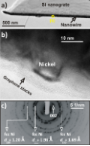
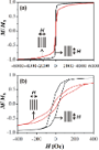
Functionalised zinc oxide nanowire gas sensors: Enhanced NO2 gas sensor response by chemical modification of nanowire surfaces
Beilstein J. Nanotechnol. 2012, 3, 368–377, doi:10.3762/bjnano.3.43
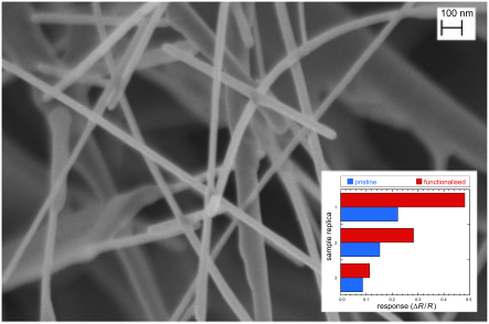
- interacted with residual oxygen to give ZnO nanowires [13]. The stabilised samples were then provided by interdigitated Pt electrodes deposited by RF magnetron sputtering, while on the back side a Pt meander was deposited to act as heater (by Joule effect) and temperature sensor. Ex situ functionalisation of



Junction formation of Cu3BiS3 investigated by Kelvin probe force microscopy and surface photovoltage measurements
Beilstein J. Nanotechnol. 2012, 3, 277–284, doi:10.3762/bjnano.3.31

- with Al, deposited by dc magnetron sputtering [21]. For analysis by Kelvin probe force microscopy (KPFM) [7], surface photovoltage (SPV), and X-ray photoemission spectroscopy (XPS), sample contact was established at the Al back contact. CdS thin films were deposited onto the Cu3BiS3 layers from a


Extended X-ray absorption fine structure of bimetallic nanoparticles
Beilstein J. Nanotechnol. 2011, 2, 237–251, doi:10.3762/bjnano.2.28
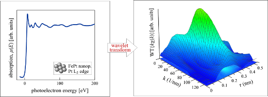
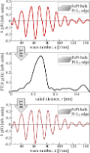
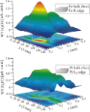
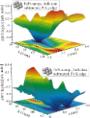
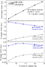
- annealing of the nanoparticles or in-flight annealing of FePt nanoparticles synthesised by condensation from the gas phase before landing onto a substrate as described below. Gas phase synthesis FePt nanoparticles can be prepared by an inert gas condensation method based on a DC magnetron sputtering process



Other Beilstein-Institut Open Science Activities