

Search results
Search for "aluminium" in Full Text gives 156 result(s) in Beilstein Journal of Nanotechnology.
Self-assembly of octadecyltrichlorosilane: Surface structures formed using different protocols of particle lithography
Beilstein J. Nanotechnol. 2012, 3, 114–122, doi:10.3762/bjnano.3.12
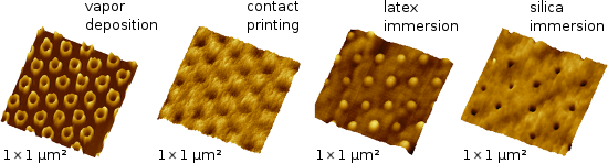
- images indicate differences in tip–surface interactions, but were not normalized for the comparison of friction changes between different tips or experiments. The tips were silicon nitride probes. Tips used with tapping-mode AFM were rectangular shaped ultrasharp silicon tips that have an aluminium




Impact of cell shape in hierarchically structured plant surfaces on the attachment of male Colorado potato beetles (Leptinotarsa decemlineata)
Beilstein J. Nanotechnol. 2012, 3, 57–64, doi:10.3762/bjnano.3.7

- commercial garden shop. Morphology The morphology of the plant surfaces was characterised by scanning electron microscopy (SEM). For investigation of epicuticular wax crystals, the samples were mounted on aluminium stubs without any prior dehydration step. For SEM analysis of cell shape and cuticular folds
- , leaf samples were dehydrated in methanol [31] and critical point dried (LPD 030, Bal-Tec). For cross-section analysis of plant surfaces, the critical-point-dried samples were cut with a razor blade. Samples were mounted on aluminium stubs by means of conductive double-sided adhesive tabs (Plano


Enhancement of the critical current density in FeO-coated MgB2 thin films at high magnetic fields
Beilstein J. Nanotechnol. 2011, 2, 809–813, doi:10.3762/bjnano.2.89

- attempts to solve the above-mentioned problem relating to the decay of the critical current in an external magnetic field. Various research teams have tried to increase the critical current density either by doping MgB2 with various substances (carbon [3], aluminium [4], etc.) or by adding nanoparticles of


Generation and agglomeration behaviour of size-selected sub-nm iron clusters as catalysts for the growth of carbon nanotubes
Beilstein J. Nanotechnol. 2011, 2, 734–739, doi:10.3762/bjnano.2.80
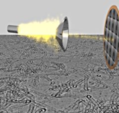
- all of the formed oxide species that are accumulated. A 10 nm Al layer was deposited prior to cluster deposition on the SiOx grid. This thin Al barrier layer later ensures CNT growth [12]. Sintering of the iron catalyst during heating is minimized due to the low Tammann temperature of aluminium (194
- °C), which prevents the iron particles from agglomeration and hence providing a good aluminium–iron interaction. Moreover, the deposited Al layer is also partially oxidized on top of the SiOx grid surface [12] and forms a stable alumina–catalyst interface, which stabilizes the deposited iron clusters
- application of a high voltage pulse to the 90° mirror, which was aligned to the target (11). The incident energy of the mass-selected clusters was 2550 eV with an energy spread of approximately 150 eV (FWHM). Chemical vapour deposition of CNTs A 10 nm thick aluminium buffer layer was deposited by means of


The effect of surface anisotropy in the slippery zone of Nepenthes alata pitchers on beetle attachment
Beilstein J. Nanotechnol. 2011, 2, 302–310, doi:10.3762/bjnano.2.35

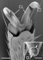
- beetles were studied in the SEM at an acceleration voltage of 3 kV. For this purpose, insects were air-dried, mounted with their dorsal side to aluminium holders, sputter-coated with gold-palladium (thickness 6 nm), and examined in SEM, as described above. The diameter of the claw tip (D) was estimated



Infrared receptors in pyrophilous (“fire loving”) insects as model for new un-cooled infrared sensors
Beilstein J. Nanotechnol. 2011, 2, 186–197, doi:10.3762/bjnano.2.22

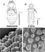
- have a significant lower absorption coefficient which requires the application of an additional absorber such as plastic, aluminium, antimony or lead [21]. When the absorbing film is directly on the inner surface of the window, the assumption of a boundary layer as in the case of water is valid


Other Beilstein-Institut Open Science Activities