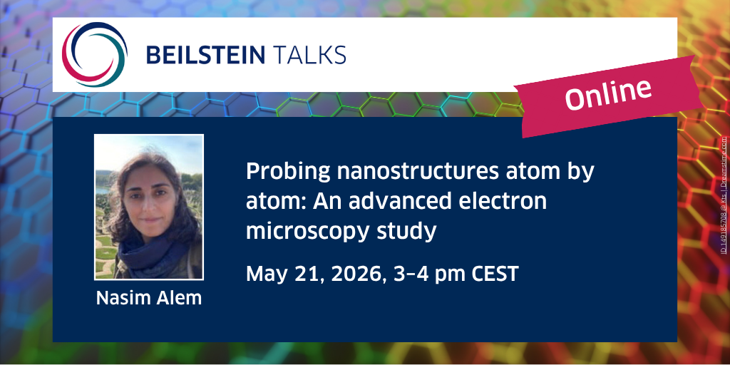
Beilstein Talk "Probing nanostructures atom by atom: An advanced electron microscopy study"
Beilstein Talks
The Beilstein Talks are an established addition to the Beilstein-Institut’s projects supporting communication and information in science. These online talks are free to attend; a simple registration is all that is required.
Probing nanostructures atom by atom: An advanced electron microscopy study
Nasim Alem / The Pennsylvania State University
May 21, 2026, 3–4 pm CEST
Online live talk
👉 Go to the free registration for the online live talk!
Introduction
In this talk, we will present our recent studies on the local electronic/atomic structure and light emission characteristics in in-plane monolayer 2D transition metal dichalcogenide (TMD) using advanced electron microscopy imaging and spectroscopy. Our studies uncover evidence of quantum confinement as well as emission of interface excitons in the dot sizes ranging from a couple of nanometers to a few tens of nanometers. This talk will also present our recent efforts in understanding the underlying physics of defect formation and heteroepitaxy in the large family of 2D vertical TMD heterostructures, which is the key in the large-scale synthesis of 2D-based heterostructure devices.
04 May 2026
Other Beilstein-Institut Open Science Activities