

Search results
Search for "electrical properties" in Full Text gives 223 result(s) in Beilstein Journal of Nanotechnology. Showing first 200.
Reliable fabrication of transparent conducting films by cascade centrifugation and Langmuir–Blodgett deposition of electrochemically exfoliated graphene
Beilstein J. Nanotechnol. 2022, 13, 666–674, doi:10.3762/bjnano.13.58
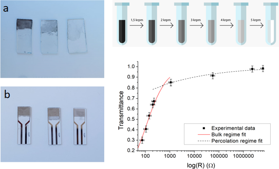
- the substrate completely. To analyze the electrical properties of the synthesized graphene films, resistance values of each film were measured. Resistance values, optical transparency values, and the average number of layers in each graphene film are shown in Table 2. A larger number of graphene


Selected properties of AlxZnyO thin films prepared by reactive pulsed magnetron sputtering using a two-element Zn/Al target
Beilstein J. Nanotechnol. 2022, 13, 344–354, doi:10.3762/bjnano.13.29
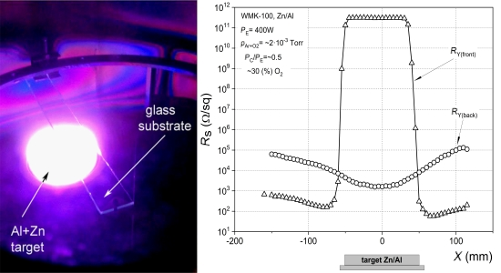
- and are then repulsed by the field near the target toward the substrate placed above it. For the case presented here, an analysis of the XRD results may be used to clarify the sudden change in the electrical properties of the deposited thin films depending on X. Measurements of structural properties



The effect of metal surface nanomorphology on the output performance of a TENG
Beilstein J. Nanotechnol. 2022, 13, 298–312, doi:10.3762/bjnano.13.25
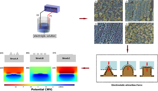
- –semiconductor and semiconductor–metal contact pairs [14][15]. A semiconductor–metal contact can be described by the band diagram shown in Figure 1. The frictional electrical properties of materials depend on their work functions and Fermi levels [16][17]. The intermediate state in the bandgap can reduce the




Investigation of a memory effect in a Au/(Ti–Cu)Ox-gradient thin film/TiAlV structure
Beilstein J. Nanotechnol. 2022, 13, 265–273, doi:10.3762/bjnano.13.21

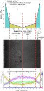
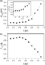
- used. All electrical measurements were made at controlled room temperature (23 °C) and humidity (30% RH) in ambient air. Results Electrical properties The resistivity of the thin film was determined to be 1 × 10³ Ω·cm. The type of electrical conductivity was determined on the basis of the sign of the



Impact of device design on the electronic and optoelectronic properties of integrated Ru-terpyridine complexes
Beilstein J. Nanotechnol. 2022, 13, 219–229, doi:10.3762/bjnano.13.16

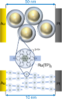
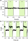
- has been successfully conducted and reveal the oxidation state of Ru during complex wire growth [19]. Electrical properties of Ru(TP)2-complex devices Here, we study the relation between device design and device performance and compare the transport and optical switching properties of functional Ru(TP


Engineered titania nanomaterials in advanced clinical applications
Beilstein J. Nanotechnol. 2022, 13, 201–218, doi:10.3762/bjnano.13.15
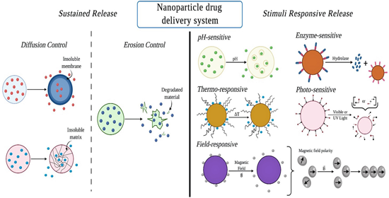
- , inorganic, or organometallic material whose chemical, physical, and/or electrical properties change as a function of the size and shape of the material. Nanomaterials are designed at the atomic or molecular level, and most of the therapeutic nanoparticles (nps) are usually between 10 and 100 nm in size so


Sputtering onto liquids: a critical review
Beilstein J. Nanotechnol. 2022, 13, 10–53, doi:10.3762/bjnano.13.2







Cantilever signature of tip detachment during contact resonance AFM
Beilstein J. Nanotechnol. 2021, 12, 1286–1296, doi:10.3762/bjnano.12.96

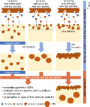
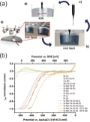
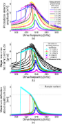
- methods provide information on important mechanical and electrical properties across a wide variety of samples. CR-AFM, PFM, and ESM are built upon the fundamental assumption that as the cantilever is excited, the probe tip remains in contact with the sample. Signal-to-noise ratios in these measurements


Plasmon-enhanced photoluminescence from TiO2 and TeO2 thin films doped by Eu3+ for optoelectronic applications
Beilstein J. Nanotechnol. 2021, 12, 1271–1278, doi:10.3762/bjnano.12.94
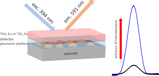
- film. However, a blueshift occurs here due to the electrical properties of aluminum oxide. Additionally, it can be seen, that the position of the minimum of transmission as function of the Al2O3 film thickness. This may be explained by the different permittivity of the layers [34][35][36]. Emission and


Two dynamic modes to streamline challenging atomic force microscopy measurements
Beilstein J. Nanotechnol. 2021, 12, 1226–1236, doi:10.3762/bjnano.12.90

- science The relative ease of use of AFM and a large number of operating modes allowed for the study of mechanical, magnetic, and electrical properties of various objects. At the same time, surface profile measurements remain both the main application of the method and the basis of two-pass technics of


Assessment of the optical and electrical properties of light-emitting diodes containing carbon-based nanostructures and plasmonic nanoparticles: a review
Beilstein J. Nanotechnol. 2021, 12, 1078–1092, doi:10.3762/bjnano.12.80
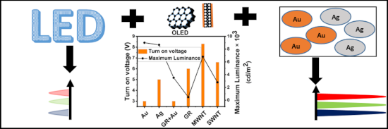
- (CNT), and graphene (GR) towards producing cost-effective and efficient LED. A second strategy consisting of enhancing the optical and electrical properties of LED via SPR of MNP is also surveyed. The LED covered in this review include inorganic LED, OLED, inorganic/organic LED, and HyLED. The
- -based ones. However, CNT and graphene tend to provide better thermal management and electrical properties; therefore, their integration into LED is of growing importance. Out of the three OLED-incorporating carbon-based nanostructures, OLED + GR possessed the lowest turn-on voltage; however, the


A Au/CuNiCoS4/p-Si photodiode: electrical and morphological characterization
Beilstein J. Nanotechnol. 2021, 12, 984–994, doi:10.3762/bjnano.12.74
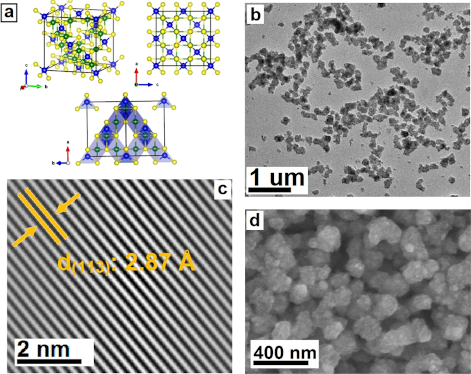
- have revealed that the bandgap value is suitable for optoelectronic devices. To the best of our knowledge, there is no study on the electrical properties of CuNiCoS4-based photodiodes. The usage of different materials as interfacial layers in metal–semiconductor devices is a hot research topic
- nanocrystals can be inserted between metal and semiconductor as interfacial layer to increase the effect of the illumination and to control electrical properties of the metal–semiconductor device. In this work, CuNiCoS4 nanocrystals were successfully obtained as interlayer of Schottky diodes. The electrical
- transition [8]. The bandgap was determined as 1.66 eV by extrapolating the linear portion of the band energy graph given in Figure 3b. Electrical properties In order to determine the electrical performance of the Au/CuNiCoS4/p-Si device, I–V measurements were performed on the photodiode in the dark and under



Impact of GaAs(100) surface preparation on EQE of AZO/Al2O3/p-GaAs photovoltaic structures
Beilstein J. Nanotechnol. 2021, 12, 578–592, doi:10.3762/bjnano.12.48
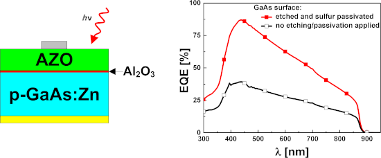
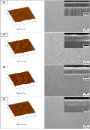
- improves optical and electrical properties of gallium arsenide-based devices [31][32][33]. In this work we examine the influence of the surface treatment of GaAs (cleaning, etching, and passivation) on the external quantum efficiency (EQE) results of the AZO/Al2O3/p-GaAs PV structures (in which AZO stands




Boosting of photocatalytic hydrogen evolution via chlorine doping of polymeric carbon nitride
Beilstein J. Nanotechnol. 2021, 12, 473–484, doi:10.3762/bjnano.12.38
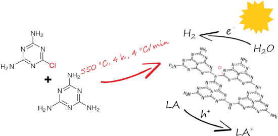
- with hydrogen evolution under simulated solar light. A series of microscopic and spectroscopic techniques have been used to characterize the morphology, chemical structure, optical, photophysical, and electrical properties of the obtained carbon nitrides. Results and Discussion The detailed analysis of


Exploring the fabrication and transfer mechanism of metallic nanostructures on carbon nanomembranes via focused electron beam induced processing
Beilstein J. Nanotechnol. 2021, 12, 319–329, doi:10.3762/bjnano.12.26

- arbitrary substrates or grids to obtain free-standing 2D membranes [25]. The specific choice of the self-assembling molecules determines the thickness, porosity, stiffness, and the mechanical/electrical properties of the resulting CNM [26][27]. The SAMs that are used for the fabrication of CNMs consist of


TiOx/Pt3Ti(111) surface-directed formation of electronically responsive supramolecular assemblies of tungsten oxide clusters
Beilstein J. Nanotechnol. 2021, 12, 203–212, doi:10.3762/bjnano.12.16
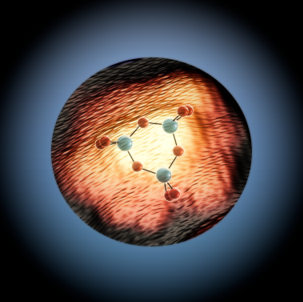
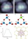
- of electronic devices appealing for the implementation in conceptually new data storage cells [1]. Specifically, resistive memories [2] based on the change of the electrical properties of a transition metal oxide thin layer, integrated in a simple electrode setup as a function of an externally



Paper-based triboelectric nanogenerators and their applications: a review
Beilstein J. Nanotechnol. 2021, 12, 151–171, doi:10.3762/bjnano.12.12
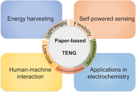
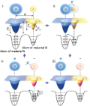
- gradual decay of the surface charges (Figure 3-iv). Treatment methods for paper and P-TENGs The electrical properties of paper are critical determinants of the performance of P-TENGs. The original paper structure usually does not meet all the requirements for the desired applications on P-TENG devices
- polydopamine to improve the output voltage of TENGs by approx. 3.5 times in comparison with unmodified TENGs. Another typical method to prepare nanoscale paper with different electrical properties is by using vacuum filtration (VF) to either obtain dielectric cellulose nanofiber (CNF)- based nanoscale paper or






A review on the green and sustainable synthesis of silver nanoparticles and one-dimensional silver nanostructures
Beilstein J. Nanotechnol. 2021, 12, 102–136, doi:10.3762/bjnano.12.9
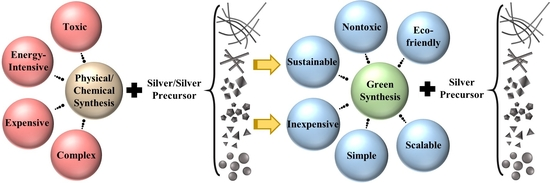
- demonstrated unique electrical properties. AgNPs coated on polycarbonate substrates were previously used to increase the electrical conductivity of polycarbonate composites [79]. AgNPs have also demonstrated minimum or no adverse effects on mechanical strength when embedded in polymeric materials or composites


ZnO and MXenes as electrode materials for supercapacitor devices
Beilstein J. Nanotechnol. 2021, 12, 49–57, doi:10.3762/bjnano.12.4
- optical and electrical properties. This review will give a prospect to researchers working on the development of electrode materials for efficient supercapacitors. The discussion of MXenes along with ZnO, although different in chemistry, also highlights the differences in dimensionality when it comes to
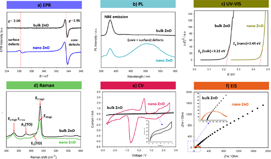
- ) spectroscopy techniques among the most powerful techniques to extract detailed information on the defect structures of ZnO. Also, electrical impedance spectroscopy (EIS) and cyclic voltammetry (CV) are sensitive to electrical properties such as specific capacitance and impedance, which can be correlated with
- mode, which is indicative of a large amount of defect centers. The existence of defect centers affects the vibration mode and eventually causes a blueshift, as shown in Figure 1d. Finally, the electrical properties obtained via CV and EIS can also be correlated with the defect structures when the
Mapping of integrated PIN diodes with a 3D architecture by scanning microwave impedance microscopy and dynamic spectroscopy
Beilstein J. Nanotechnol. 2020, 11, 1764–1775, doi:10.3762/bjnano.11.159

- microscopy (sMIM). sMIM allows for the characterization of the local electrical properties through the analysis of the microwave impedance of the metal–insulator–semiconductor nanocapacitor (nano-MIS capacitor) that is formed by tip and sample. A highly integrated monolithic silicon PIN diode with a 3D
- crucial to optimize and increase the device integration. In order to map the electrical properties of microelectronic materials with a high spatial resolution, scanning probe microscopy (SPM), based on atomic force microscopy (AFM), offers several modes based on the control of electrical conduction and on
- modes provide sub-10 nm two-dimensional maps of the electrical properties of doped semiconductor layers [1][6][7][8] when a fixed bias is applied to the nanoscale contact. In SSRM, a DC voltage is applied to the sample and the resulting current, flowing from the conductive tip through the sample to the


PEG/PEI-functionalized single-walled carbon nanotubes as delivery carriers for doxorubicin: synthesis, characterization, and in vitro evaluation
Beilstein J. Nanotechnol. 2020, 11, 1728–1741, doi:10.3762/bjnano.11.155
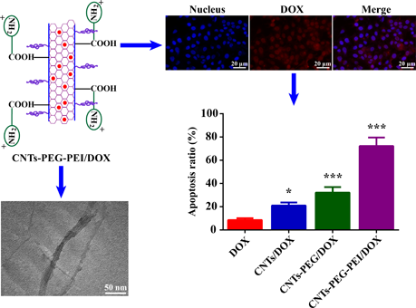
- their unique properties, including large surface area, relatively low density, high stability and other inherent mechanical, optical and electrical properties [7][8][9]. CNTs can be produced as single-walled CNTs (SWCNTs) or multi-walled CNTs (MWCNTs) [10]. SWCNTs can be easily synthesized and

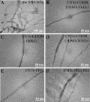
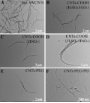

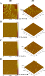
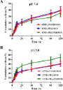


High-responsivity hybrid α-Ag2S/Si photodetector prepared by pulsed laser ablation in liquid
Beilstein J. Nanotechnol. 2020, 11, 1596–1607, doi:10.3762/bjnano.11.142

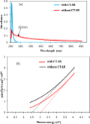
- –S bonds and the second-order longitudinal optical phonon 2LO mode; their intensity increased when CTAB was added to Tu. FTIR data revealed the presence of a Ag–S bond located at 510 cm−1. The electrical properties of the Ag2S/Si heterojunction were significantly enhanced after the addition of CTAB




Structural and electronic properties of SnO2 doped with non-metal elements
Beilstein J. Nanotechnol. 2020, 11, 1321–1328, doi:10.3762/bjnano.11.116
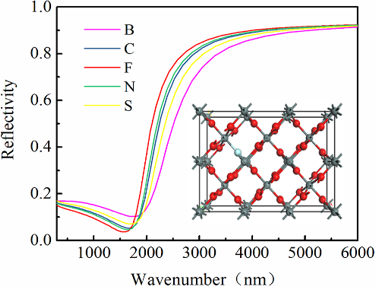
- preferred orientation, optical properties, and electrical properties of SnO2 film are improved. Analysis of the electrical properties of SnO2 films doped with different non-metal elements showed that the resistance of SnO2 films doped with N was higher [6][7][8] than that of SnO2 doped with other elements
- successfully prepared from N-doped SnO2 films. Through Al/N co-doping, a p-type SnO2 semiconductor thin film with excellent electrical properties was prepared. The resistivity, hole concentration and hole mobility were 7.1 × 10⁻³ Ω·cm, 6.24 × 1019 cm−3 and 14.1 cm2·V−1·s−1, respectively [8]. Doping SnO2 with F
- performance of SnO2 is not yet clear. In recent years, many researchers used first-principles calculations to scrutinize the doping of SnO2 with non-metal elements such as F [11][12] and S [13]. The results show that the optical and electrical properties of SnO2 thin films can be changed by doping with



Magnetohydrodynamic stagnation point on a Casson nanofluid flow over a radially stretching sheet
Beilstein J. Nanotechnol. 2020, 11, 1303–1315, doi:10.3762/bjnano.11.114

- FORTRAN. Nanoparticles have unique thermal and electrical properties which can improve heat transfer in nanofluids. The effects of pertinent flow parameters on the nondimensional velocity, temperature and concentration profiles are presented. Overall, the results show that the heat transfer rate increases


An atomic force microscope integrated with a helium ion microscope for correlative nanoscale characterization
Beilstein J. Nanotechnol. 2020, 11, 1272–1279, doi:10.3762/bjnano.11.111

- [24] with very high resolution. Magnetic properties of nanostructures can be measured using magnetic force microscopy (MFM) [42], and a host of AFM techniques are available to measure electrical properties of samples (e.g., conductive AFM (cAFM) [43], scanning capacitance microscopy (SCM) [44], and