

Search results
Search for "exciton" in Full Text gives 106 result(s) in Beilstein Journal of Nanotechnology.
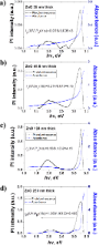
Observing the morphology of single-layered embedded silicon nanocrystals by using temperature-stable TEM membranes
Beilstein J. Nanotechnol. 2015, 6, 964–970, doi:10.3762/bjnano.6.99

- distance and density regardless of the application [11][12][13]. Moreover, there is compelling evidence of multiple exciton generation in adjacent Si NCs with almost ideal quantum efficiencies which is explained in terms of space-separated quantum cutting due to strong coupling between neighboring Si NCs


Effects of swift heavy ion irradiation on structural, optical and photocatalytic properties of ZnO–CuO nanocomposites prepared by carbothermal evaporation method
Beilstein J. Nanotechnol. 2015, 6, 928–937, doi:10.3762/bjnano.6.96
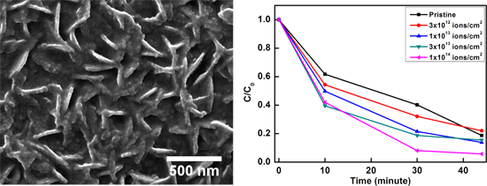
- gap and large exciton binding energy, making it suitable for a wide range of applications such as UV lasers [11], dye-sensitized solar cells [12][13][14], gas sensors [15][16], UV sensors [17], light emitting diodes [18], spintronic devices [19], transparent conductive electrodes [20], lasers [21


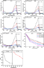
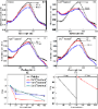

Morphology control of zinc oxide films via polysaccharide-mediated, low temperature, chemical bath deposition
Beilstein J. Nanotechnol. 2015, 6, 799–808, doi:10.3762/bjnano.6.83

- material with a direct band gap of 3.37 eV and an exciton binding energy of 60 meV [19]. Although ZnO is reported to be an n-type semiconductor (most likely due to the hydrogen impurities which act as shallow donors), it is a challenging task to control its conductivity [20]. In general, in applications




Carrier multiplication in silicon nanocrystals: ab initio results
Beilstein J. Nanotechnol. 2015, 6, 343–352, doi:10.3762/bjnano.6.33

- ] and, in some cases, (c) by the so-called “phonon bottleneck” effect [9][10] that reduces the probability of exciton relaxation by phonon emission. These conditions make the formation of multiple e–h pairs after absorption of high energy photons more likely to occur in low-dimensional nanostructures
- . Therefore, in our opinion, more complicated dynamics, where for instance SSQC effects are assisted by exciton recycling mechanisms [31][41], must be hypothesized in order to explain results of [36]. Conclusion In this work, we have calculated CM lifetimes for systems of isolated and interacting Si-NCs. As a


![[Graphic 31]](/bjnano/content/inline/2190-4286-6-33-i39.png?max-width=637&scale=1.18182) is given in the upper part of the figure. ...
is given in the upper part of the figure. ...
Nanoporous Ge thin film production combining Ge sputtering and dopant implantation
Beilstein J. Nanotechnol. 2015, 6, 336–342, doi:10.3762/bjnano.6.32
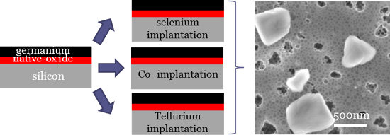
- applications, since they can lead to multiple exciton generation [7]. In particular, multiple exciton generation has been previously demonstrated in Si nanostructures [8]. Ge has a similar structure to Si, however, it offers several benefits compared to Si such as faster carrier mobility, smaller band gap and
- lower process temperatures [9]. In addition, the Ge exciton Bohr radius (≈24 nm) is significantly larger than that of Si (≈4.5 nm), allowing for quantum effects to appear in nanostructures exhibiting larger sizes [10], and allowing the k-selection rules to be broken. For example, lasing has only been
- the pores, allowing for the production of Ge nanoporous films exhibiting characteristic skeleton sizes smaller (≈10 nm, without annealing) or larger (≈50 nm, annealing at 675 °C for 1 h) than the Ge-exciton Bohr radius, depending on the desired applications. Experimental The Ge layers were deposited


Bright photoluminescence from ordered arrays of SiGe nanowires grown on Si(111)
Beilstein J. Nanotechnol. 2014, 5, 2498–2504, doi:10.3762/bjnano.5.259

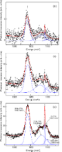
- . In order of increasing energy, they are readily assigned to the NW free-exciton transverse-optic (TO) Si–Si vibrational mode, NW free-exciton transverse-acoustic (TA) phonon, Si–substrate-bound-exciton TO phonon and NW free-exciton no-phonon (NP) lines, respectively [31][35]. The peak amplitude data
- -exciton NP line intensity relative to its phonon replicas (TA and TO lines) in these NWs is much more intense than that found in bulk Si, but is somewhat lower compared to what is observed in bulk alloy material of a similar composition [35], which may reflect on the action of NW surface effects as
- well with the values expected for bulk Si1−xGex with x = 0.15 of 18 (1) and 58 meV, respectively [35]. The measured NW free-exciton NP energy of 1099 meV would indicate a Ge concentration of x = 0.14 (this concentration gives an X-point energy gap of 1099 meV in bulk SiGe) [35]. Thus the positions in


Silicon and germanium nanocrystals: properties and characterization
Beilstein J. Nanotechnol. 2014, 5, 1787–1794, doi:10.3762/bjnano.5.189
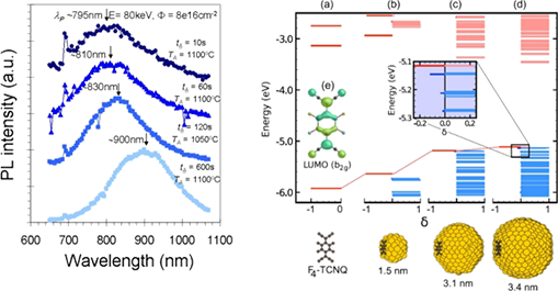
- effects is important especially for small nanoparticles in which the exciton binding energy can be large [55]. These can be calculated by using the Bethe–Salpeter equation [7]. However, for nanocrystals with a radius larger than 0.6 nm, the self-energy and the Coulomb corrections almost exactly cancel


Effects of palladium on the optical and hydrogen sensing characteristics of Pd-doped ZnO nanoparticles
Beilstein J. Nanotechnol. 2014, 5, 1261–1267, doi:10.3762/bjnano.5.140

- green luminescence band originates from palladium ions, which replace zinc and always occur in ZnO in a small amount. The dominant peak at 517 nm corresponds to the exciton transition from the ground-state electronic subband to the ground-state of Pd in replacing Zn sites (i.e., PdZn vacancies). The
- excited state of PdZn originates from a hole bound to 4d10 shells or an intermediately bound exciton to a neutral d9 configuration due to the hybridization of the Pd4d states with the Zn4s states at the bottom of the conduction band. The electron capture takes place at the neutral PdZn center (i.e., [Pd2


An insight into the mechanism of charge-transfer of hybrid polymer:ternary/quaternary chalcopyrite colloidal nanocrystals
Beilstein J. Nanotechnol. 2014, 5, 1235–1244, doi:10.3762/bjnano.5.137
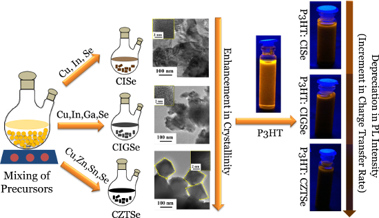
- polymer and acceptor chalcopyrite has to be sufficiently fast to their respective electrodes in order to avoid non-radiative recombination, which can occur at the interface between the two materials and can therefore alter the device photocurrent [24]. However, after successful exciton dissociation across
- across the donor–acceptor interface another possible mechanism of charge transportation could be energy transfer, i.e., the Forster resonance energy transfer (FRET) from the donor to the acceptor after excitation, which results in the generation of an exciton in the acceptor. This mechanism, however, can


Functionalized nanostructures for enhanced photocatalytic performance under solar light
Beilstein J. Nanotechnol. 2014, 5, 994–1004, doi:10.3762/bjnano.5.113
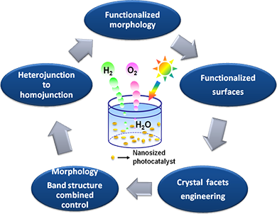
- high crystallinity, high surface area and unique microstructure [63]. As the crystal size of the semiconductor is close to the exciton Bohr radius, its bandgap can be enlarged with a reduced crystal size due to the quantum confinement effect. Therefore, we have synthesized Co3O4 quantum dots (3–4 nm


Optical and structural characterization of oleic acid-stabilized CdTe nanocrystals for solution thin film processing
Beilstein J. Nanotechnol. 2014, 5, 881–886, doi:10.3762/bjnano.5.100

- such as multiple exciton generation [16]. In the last years, nanostructured semiconductors have proved to be useful as raw material for solution-processable electronic technologies. The capping of semiconductor nanocrystals by organic ligands, provides the control of composition, size, shape and
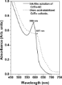
- lower than the exciton Bohr radius of the bulk counterpart. In the case of CdTe, the reported parameter is 6.8 nm [42], whilst the CdTe crystal size was 3.5 nm, as estimated from TEM and XRD measurements. The absorbance spectra shown in Figure 5 exhibit a well-defined peak in the visible wavelength
- distribution for our samples. Nevertheless the exciton peak disappeared once the CdTe colloid was drop-cast on the glass substrates Figure 5 shows the absorbance spectra of CdTe-NC of the colloidal solution and of a liquid sample processed by the size-separation technique. The effect of size-separation can be


Preparation of poly(N-vinylpyrrolidone)-stabilized ZnO colloid nanoparticles
Beilstein J. Nanotechnol. 2014, 5, 402–406, doi:10.3762/bjnano.5.47
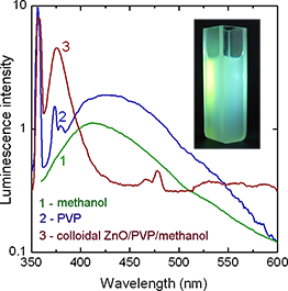
- from the most intense PL band at 356 nm coming from the PVP, exhibits a strong PL band at 376 nm (3.30 eV) which corresponds to the emission of the free exciton recombination in ZnO nanoparticles. Keywords: colloidal solutions; nanocomposite; poly(N-vinylpyrrolidone); sol–gel; zinc oxide
- -bandgap luminescence with a maximum at 376 nm, which coincides with that observed in high-quality ZnO bulk crystals and is related to the recombination of free excitons. The observation of efficient free exciton emission at room temperature, as well as the weak visible emission observed at 550 nm is
- corresponds to the emission from the free exciton recombination in ZnO nanoparticles. The position of this emission band coincides with the one related to free exiton recombination in ZnO microwires [18]. Note, that if we will add the value of the free exciton binding energy of 60 meV to the position of this


Photoactivation of luminescence in CdS nanocrystals
Beilstein J. Nanotechnol. 2014, 5, 355–359, doi:10.3762/bjnano.5.40
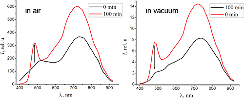
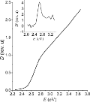
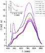
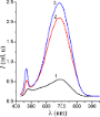
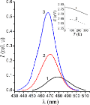
- fluorescence enhancement (PFE) [1][2][3][4][5], intermittency or blinking of photoluminescence [6][7][8], and a blue- or red-shift of the exciton PL of nanocrystals [5][9]. Despite the large number of works devoted to the surface interactions in II–IV QDs [2][3][4][5][10] the mechanisms responsible for the
- mainly related to a single exciton emission band. Therefore, it is interesting to study the luminescent properties of quantum dots of other materials and other matrices that contain the QDs. Unlike [1][2][4][5] this paper investigates the luminescence of cadmium sulfide nanocrystals dispersed in a
- intensity of luminescence bands, which differs from the results described in [1]. In [1] an increase in the intensity of the exciton band is accompanied by a simultaneous decrease in the intensity of the "defective" luminescence band. In our experiments, we observed no shift of the maximum short-wavelength


Study of mesoporous CdS-quantum-dot-sensitized TiO2 films by using X-ray photoelectron spectroscopy and AFM
Beilstein J. Nanotechnol. 2014, 5, 68–76, doi:10.3762/bjnano.5.6

- -CdS and TiO2 is due to the different energy levels of the different conduction and valence bands [7]. This transfer takes place if an exciton is generated by the absorption of an incident photon. If the conduction band energy of CdS is higher than that of TiO2 the electron can be ejected [6]. Several
- sensitize TiO2. The suitable positions of the potential energies allow for an easy transfer of the exciton between the semiconductors. Not only does that help to optimize the charge separation by reducing the recombination of charges, it also allows for an extension of the photoresponse of the photocatalyst


Many-body effects in semiconducting single-wall silicon nanotubes
Beilstein J. Nanotechnol. 2014, 5, 19–25, doi:10.3762/bjnano.5.2

- [57]. As illustrated later, the exciton binding energy compensates the discrepancy between the electronic band gap calculated by DFT and the optical gap observed experimentally. As a representation, electronic wave functions of the last valence band and the first conduction band of (4,4) SiNT at the k
- case of (10,0) SiNT. The smaller binding energy of the bright exciton in (10,0) SiNT is probably a consequence of the smaller quasi-electron effective mass. Since the interband transitions between the last valence band and the first conduction band are dipole-forbidden, there are several dark
- (optically inactive) excitons below the bound exciton in (10,0) SiNT. Compared with two-dimensional silicene, excitonic effects in SiNTs are stronger due to the lower dimensionality. The BS two-particle’s Hamiltonian was diagonalized to obtain the e−h wave functions (quantum amplitudes) to show the


Evolution of microstructure and related optical properties of ZnO grown by atomic layer deposition
Beilstein J. Nanotechnol. 2013, 4, 690–698, doi:10.3762/bjnano.4.78
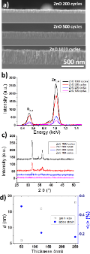
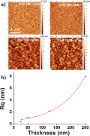
- (3.36 eV), a high dielectric constant, a high exciton binding energy (60 meV), and a high thermal stability [1]. Hence it is an important material for different applications in devices such as gas sensors [2], biosensors [3], transducers [4], solar cells [5][6][7], electronic and optoelectronic
- range and a broad emission band in the range of 480–620 nm [23][24][25]. The UV emission band in ZnO has been related to exciton emission, whereas the vis emission has been related to radiative transitions involving intrinsic point defects (O/Zn vacancies and O/Zn interstitials) [23][24][25]. ALD is an
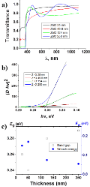
- state-valence band and the defect state-conduction band (Figure 4a–d) [49][50][51][52]. The binding energy of free exciton in ZnO is 0.06 eV. The exciton emission energy Ex and the energy gap Eg are correlated [53]: where, Eb , ћ, k, mex are the exciton binding energy, Planck’s constant, wave vector

Optimization of solution-processed oligothiophene:fullerene based organic solar cells by using solvent additives
Beilstein J. Nanotechnol. 2013, 4, 680–689, doi:10.3762/bjnano.4.77

- that during vacuum deposition the evaporation rate and substrate temperature can be precisely controlled and may be optimized to create highly ordered domains of donor and acceptor material [41]. These crystalline domains allow for higher exciton diffusion lengths [42] and thus higher charge generation


High-resolution electrical and chemical characterization of nm-scale organic and inorganic devices
Beilstein J. Nanotechnol. 2013, 4, 318–319, doi:10.3762/bjnano.4.35
- reduced exciton diffusion lengths (and thus more efficient collection) through the fabrication of an entangled mixture of the acceptor–donor layers, the addition of light scattering nanoparticles or metallic nanoparticles (spectrum harvesting through plasmonics) in the active layer or even wavelength
Photoresponse from single upright-standing ZnO nanorods explored by photoconductive AFM
Beilstein J. Nanotechnol. 2013, 4, 208–217, doi:10.3762/bjnano.4.21

- temperature) and high exciton binding energy (60 meV) and being piezoelectric, ZnO is one of the most promising semiconductor materials. Fields of application include solar cells [1][2][3][4], piezo-actuators [5], energy harvesting devices [6], and photosensors [7][8][9][10][11][12][13][14][15][16]. A common
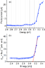
- commonly attributed to the presence of oxygen vacancies [17]. The crystalline quality can be estimated by a simple comparison of the intensities of the exciton peak and defect band. From the PL measurements we conclude that the generation of electron–hole pairs at room temperature becomes possible with a



Horizontal versus vertical charge and energy transfer in hybrid assemblies of semiconductor nanoparticles
Beilstein J. Nanotechnol. 2012, 3, 629–636, doi:10.3762/bjnano.3.72

- type of transfer process. Wu et al. studied charge separation in type-II heterojunction assemblies of CdSe–CdTe NPs as a function of linker length [23]. They found that for longer linkers, the charge transfer efficiency is smaller. In another study, photogenerated exciton dissociation in PbS NP thin
- an exciton by the Dexter mechanism [39]. Hence, the Dexter transfer rate is proportional to the simultaneous tunneling of electrons and holes. The main differences between the Förster and Dexter mechanisms is that the Dexter mechanism demands an orbital overlap, between the donor and acceptor
- acceptors being charged, until charge recombination occurs. As long as these NPs are charged, the charge or exciton transfer (in the Dexter mechanism the electron and hole are transferred simultaneously) is less efficient to them due to the Columbic repulsion, which results in a reduction in the overlap of


Low-temperature synthesis of carbon nanotubes on indium tin oxide electrodes for organic solar cells
Beilstein J. Nanotechnol. 2012, 3, 524–532, doi:10.3762/bjnano.3.60

- the fullerene derivative acts as an electron acceptor [6]. The holes move in the polymeric phase towards the anode, while the electrons hop along the fullerenes and eventually reach the cathode. Since the diffusion length of the exciton in the polymers is very low, recombination is highly probable
- , unless the electron is quickly injected into the carbon (acceptor) phase. Unfortunately, the concurrence of a low electrical mobility (due to the hopping mechanism) with a small exciton diffusion length increases the likelihood of charge recombination, ultimately affecting the overall PCE of the cells [7
- with a large interface area over which a strong electric field would lead to a high probability of exciton dissociation [16]. However, the lack of control over the selection of the CNTs has made their integration with polymers quite unsuccessful so far [17], as recently suggested by photoluminescence




Effect of deposition temperature on the structural and optical properties of chemically prepared nanocrystalline lead selenide thin films
Beilstein J. Nanotechnol. 2012, 3, 438–443, doi:10.3762/bjnano.3.50

- ; optical absorption; Introduction Lead selenide (PbSe) with its narrow band gap (Eg = 0.27 eV) [1] is an important semiconductor of the IV–VI lead chalcogenides group. PbSe has a large exciton Bohr radius (46 nm), which offers the opportunity to achieve strong size quantization at relatively large crystal




Ultraviolet photodetection of flexible ZnO nanowire sheets in polydimethylsiloxane polymer
Beilstein J. Nanotechnol. 2012, 3, 353–359, doi:10.3762/bjnano.3.41

- photoresponse. Keywords: permeable polymer; photoresponse; polydimethylsiloxane; UV photodetection; ZnO nanowires; Introduction ZnO is a direct wide band gap semiconductor with a 3.37 eV gap and a high exciton binding energy of 60 meV at room temperature, which is promising for optoelectronic applications


X-ray absorption spectroscopy by full-field X-ray microscopy of a thin graphite flake: Imaging and electronic structure via the carbon K-edge
Beilstein J. Nanotechnol. 2012, 3, 345–350, doi:10.3762/bjnano.3.39
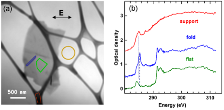
- near 292 eV corresponds to the σ* threshold. This peak is composed of two distinct features at 291.5 eV and 292.6 eV. The sharp feature at 291.5 eV is an exciton [24], its sharpness reflecting the strong correlation effects of electron–hole pairs within the flake. The broad peak at 292.6 eV is related



Optical properties of fully conjugated cyclo[n]thiophenes – An experimental and theoretical approach
Beilstein J. Nanotechnol. 2011, 2, 720–726, doi:10.3762/bjnano.2.78

- based on a Frenkel exciton Hamiltonian. Furthermore, intriguing new bands in the absorption and fluorescence spectra of the smaller macrocycles disclose the dominance of their ring strain. Keywords: conjugated macrocycles; Frenkel exciton model; oligothiophene; photophysical properties; Introduction
- the solubilizing butyl side chains. The obtained structure–property relationships were further analyzed by our theoretical model based on Frenkel exciton theory. The comparison of the experimental with the theoretical spectral parameters gave valuable insights into the electronic structure, because
- fixed value with increasing size of the macrocycle. The size-dependent effects on the absorption spectra (energy and extinction coefficient) can be described in the framework of a Frenkel exciton theory. The small macrocycles show most interesting photophysical behaviour (dual fluorescence), mostly due