
Search results
Search for "annealing" in Full Text gives 501 result(s) in Beilstein Journal of Nanotechnology. Showing first 200.
Scanning tunneling microscopy and spectroscopy of rubrene on clean and graphene-covered metal surfaces
Beilstein J. Nanotechnol. 2020, 11, 1157–1167, doi:10.3762/bjnano.11.100
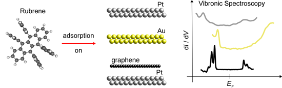
- surface. Experimental The experiments were performed with an STM operated in ultrahigh vacuum (10−9 Pa) and at low temperature (Pt(111) and graphene-covered Pt(111) at 5 K, Au(111) at 78 K). Pt(111) and Au(111) surfaces were cleaned by Ar+ ion bombardment and annealing. Graphene was epitaxially grown on
- backbones were presented in [25][26][27][34] for Au(111) and in [35] for Bi(111). In these reports, the deposition of molecules was performed at 5 K [25][26][27][34] and 100 K [35] with subsequent annealing at room temperature [25][26][27][34] and 350 K [35]. Therefore, deposition at low temperature seems
- to favor the adsorption with twisted and tilted backbones, possibly due to an initial high density of small island with chiral molecules, while the subsequent annealing preserves the twisted and tilted configuration of the molecular backbone and leads to homochiral domains. The twisted configuration



Monolayers of MoS2 on Ag(111) as decoupling layers for organic molecules: resolution of electronic and vibronic states of TCNQ
Beilstein J. Nanotechnol. 2020, 11, 1062–1071, doi:10.3762/bjnano.11.91

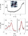
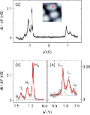
- vibronic states of the gas-phase molecule. Results and Discussion We have grown monolayer islands of MoS2 on an atomically clean Ag(111) surface, which had been exposed to sputtering–annealing cycles under ultrahigh vacuum before. The growth procedure was adapted from that of MoS2 on Au(111) [34][35], with


Highly sensitive detection of estradiol by a SERS sensor based on TiO2 covered with gold nanoparticles
Beilstein J. Nanotechnol. 2020, 11, 1026–1035, doi:10.3762/bjnano.11.87
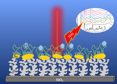
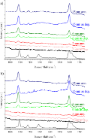
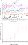
- . Specifically, we demonstrate that the TiO2 background pressure during pulsed laser deposition and the annealing conditions offer control over the formation of Au nanoparticles with different sizes, shapes and distributions, yielding a versatile sensor. We have exploited the surface for the detection of 17β
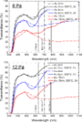
- quartz microbalance sensor. Three different values of Au thickness, namely 3, 6, and 15 nm, were selected enabling the formation of different sizes of AuNPs through subsequent annealing. Selected samples underwent annealing at 500 °C for 2 h in air, in a Lenton muffle furnace with 4 °C/min heating ramp
- top of the TiO2 films. Three nominal thickness values of 3, 6, and 15 nm were chosen, in order to obtain NPs with different diameters (Table 1). After deposition of Au, samples underwent an annealing treatment in a furnace at 500 °C for 2 h, which leads to the crystallization of TiO2 to the anatase



Gas-sensing features of nanostructured tellurium thin films
Beilstein J. Nanotechnol. 2020, 11, 1010–1018, doi:10.3762/bjnano.11.85
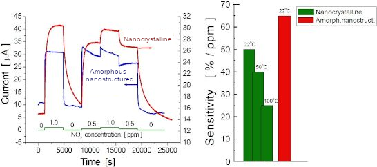
- both the heating and the annealing of the samples, the test cell was mounted inside a furnace. A platinum temperature detector (PT-100, Cliptec Kabeltechnik, Germany) was placed close to the film and was used to assist with the temperature control. The data was processed using a PC equipped with a data


Band tail state related photoluminescence and photoresponse of ZnMgO solid solution nanostructured films
Beilstein J. Nanotechnol. 2020, 11, 899–910, doi:10.3762/bjnano.11.75
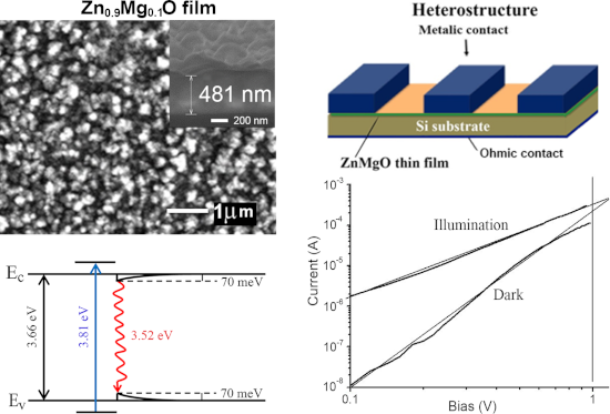
- emission properties were studied by photoluminescence spectroscopy under excitation at 325 nm. It was found that annealing at 500 °C leads to the production of macroscopically homogeneous wurtzite phase films, while thermal treatment at higher or lower temperature results in the degradation of the
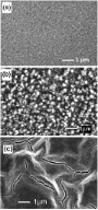
- deposited by spin coating and subjected to post-deposition annealing at 400 °C and 500 °C is similar. However, the morphology degrades for films annealed at temperatures higher than 600 °C. Figure 2 compares the surface morphology of films prepared by aerosol spray pyrolysis and spin coating annealed at 500
- . At the same time, the annealing of films at 650 °C (see Figure 2c) leads to deterioration of the morphology resulting in numerous cracks. We suppose that the difference in roughness of films prepared by the two methods is determined by the specific features of the technology. Namely, the deposition

Adsorption behavior of tin phthalocyanine onto the (110) face of rutile TiO2
Beilstein J. Nanotechnol. 2020, 11, 821–828, doi:10.3762/bjnano.11.67

- molecules into the Sn-down conformation was observed either after sample annealing at 200 °C or as a result of tip-induced manipulation. Room-temperature measurements conducted for a coverage of close to a monolayer showed no tendency for molecular arrangement. Keywords: rutile (110) surface; scanning
- the position of a tin atom protruding from the macrocycle: “Sn-up” and “Sn-down”. Switching from the Sn-up to the Sn-down geometry can be realized by annealing the sample at 200 °C or by tip-induced manipulation (bias pulse). X-ray photoelectron spectroscopy (XPS) measurements reveal a lack of strong
- prepared by repetitive cycles of Ar+-ion bombardment at an energy of 1 keV and subsequent annealing to a temperature of 700 °C. Tin phthalocyanine molecules (Tokyo Chemical Industry Co., Ltd.) were thermally evaporated by using an effusion cell (Kentax GmbH). After prudent degassing, the deposition flux


Epitaxial growth and superconducting properties of thin-film PdFe/VN and VN/PdFe bilayers on MgO(001) substrates
Beilstein J. Nanotechnol. 2020, 11, 807–813, doi:10.3762/bjnano.11.65

- , Germany). LEED images were taken of the pristine MgO(001) substrate after annealing (Figure 1a), after the deposition of VN(30 nm) on MgO (Figure 1b), after the deposition of Pd0.92Fe0.08 on VN (Figure 1c) and after the deposition of VN on Pd0.96Fe0.04 (Figure 1d). Figure 1b indicates that the individual


Hexagonal boron nitride: a review of the emerging material platform for single-photon sources and the spin–photon interface
Beilstein J. Nanotechnol. 2020, 11, 740–769, doi:10.3762/bjnano.11.61
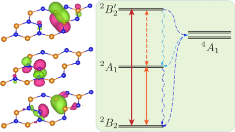
- brightest SPSs observed in any material at room temperature. Similarly, bulk BN was studied by [100] after annealing the sample in Ar at 850 °C for 30 min and at 0.5 Torr to increase the concentration of defects with similar ZPLs previously reported. However, they were found to photo-bleach with excitation
- density of emitters. Such methods based on high-temperature annealing in air and ultraviolet ozone processing are effectively used to improve SP purity (g(2)(0) ≤ 0.1) and the linewidth (FWHM room temperature of ≈3 nm) of the ZPL of CVD-grown h-BN [108]. By control of the boron diffusion through copper
- with 10 keV gallium ions at a dose of 10−14 C/µm2 with subsequent annealing with argon at 1 Torr and 750 °C for 30 min. The lifetime, brightness, and PL stability of this SPE are similar to those in 2D h-BN, however with a wavelength variation smaller by a factor of five as compared to the SPEs in 2D h




Structural optical and electrical properties of a transparent conductive ITO/Al–Ag/ITO multilayer contact
Beilstein J. Nanotechnol. 2020, 11, 695–702, doi:10.3762/bjnano.11.57
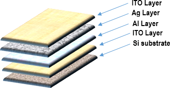
- pure ITO layer (as reference) were prepared by RF and DC sputtering. The microstructural, optical and electrical properties of the ITO/Al–Ag/ITO (IAAI) films were investigated before and after annealing at 400 °C. X-ray diffraction measurements show that the insertion of the Al–Ag intermediate bilayer
- led to the crystallization of an Ag interlayer even at the as-deposited stage. Peaks attributed to ITO(222), Ag(111) and Al(200) were observed after annealing, indicating an enhancement in crystallinity of the multilayer films. The annealed IAAI film exhibited a remarkable improvement in optical
- × 10−3 Ω−1). These highly conductive and transparent ITO films with Al–Ag interlayer can be a promising contact for low-resistance optoelectronics devices. Keywords: annealing; DC sputtering; figure of merit; indium tin oxide (ITO); multilayer structure; RF sputtering; Introduction Transparent


Soybean-derived blue photoluminescent carbon dots
Beilstein J. Nanotechnol. 2020, 11, 606–619, doi:10.3762/bjnano.11.48
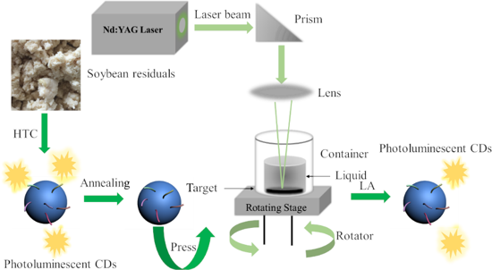
- residuals to synthesize carbon nanoparticles by hydrothermal carbonization (HTC), annealing at high temperature, and laser ablation (LA) in a NH4OH solution. The carbon nanoparticles synthesized with the HTC process (HTC-CDs) exhibit photoluminescent characteristics with strong blue emission. The annealing
- , which involves the HTC treatment, high-temperature annealing, and LAL processing, sequentially. The purpose of the LAL processing is to introduce N-containing functional groups onto the surface of carbon nanoparticles and to recover the PL of carbon nanoparticles/CDs that was quenched by the high
- -temperature annealing. Both methods can be categorized as top-down methods in contrast to bottom-up methods. The PL characteristics of the CDs produced by both methods are analyzed, and the PL mechanisms of the CDs are discussed. The strategies developed in this work offer simple and effective means for


Correction: Photocatalytic antibacterial performance of TiO2 and Ag-doped TiO2 against S. aureus. P. aeruginosa and E. coli
Beilstein J. Nanotechnol. 2020, 11, 547–549, doi:10.3762/bjnano.11.43
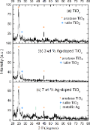
- relating to Ag, although very low intensity peaks related to Ag were observed for the sample calcined at 600 °C [6]. In a previous work, it was found that the intensity of the anatase peaks decreased in comparison to the rutile peaks as the annealing temperature increased; and after annealing at 800 °C
Evolution of Ag nanostructures created from thin films: UV–vis absorption and its theoretical predictions
Beilstein J. Nanotechnol. 2020, 11, 494–507, doi:10.3762/bjnano.11.40

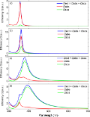
- Narutowicza 11/12, 80-233 Gdansk, Poland 10.3762/bjnano.11.40 Abstract Ag-based plasmonic nanostructures were manufactured by thermal annealing of thin metallic films. Structure and morphology were studied using scanning electron microscopy (SEM), transmission electron microscopy (TEM), high-resolution
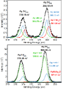
- transmission electron microscopy (HR-TEM) and X-ray photoelectron spectroscopy (XPS). SEM images show that the formation of nanostructures is influenced by the initial layer thickness as well as the temperature and the time of annealing. The Ag 3d and Ag 4d XPS spectra are characteristic of nanostructures. The
- . However, in the case of very simple production methods, as wet chemical synthesis or dewetting, the size of the nanoparticles follows a Gaussian distribution. This work focusses on Ag-based plasmonic platforms manufactured by thermal annealing of thin metallic films. The experimental results are




Atomic-resolution imaging of rutile TiO2(110)-(1 × 2) reconstructed surface by non-contact atomic force microscopy
Beilstein J. Nanotechnol. 2020, 11, 443–449, doi:10.3762/bjnano.11.35
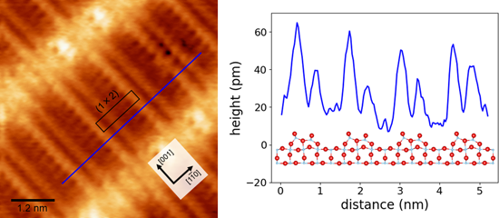
- .) were used. A rutile TiO2(110)-(1 × 2) reconstructed surface was prepared by iterating a surface cleaning process of Ar+ sputtering (2 keV, Ar partial pressure of 3.0 × 10⁻⁴ Pa, ion current of ca. 1.1 µA, 10 min) and annealing (substrate temperature of ca. 1000 °C, 30 min). STM and NC-AFM imaging was


Facile biogenic fabrication of hydroxyapatite nanorods using cuttlefish bone and their bactericidal and biocompatibility study
Beilstein J. Nanotechnol. 2020, 11, 285–295, doi:10.3762/bjnano.11.21
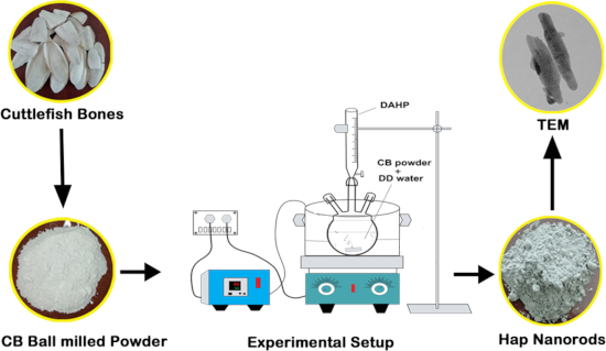
- in the crystallite size will lead to reduction in the mechanical properties of the Hap nanoparticles [36]. Moreover, Ooi et al. (2018) recently reported that a high annealing temperature will affect the porous structure of Hap nanoparticles [37]. In the present study, the TGA (Figure 3) shows 0
- % weight loss at 600 °C to form CB-Hap NRs due to the complete removal of organic substances and water. Thus, 700 °C is selected as the optimum annealing temperature for the formation of Hap NRs as suggested from previous studies. Morphology and elemental analysis TEM micrographs of CB-derived Hap nanorods
- after annealing which may be due to the removal of organic products such as collagen and protein. Chemicals and reagents Marine waste cuttlefish bones were collected as a source of calcium from Kasimedu fish market, which is located in Chennai, Tamil Nadu, India. All chemicals used for this study were




High-performance asymmetric supercapacitor made of NiMoO4 nanorods@Co3O4 on a cellulose-based carbon aerogel
Beilstein J. Nanotechnol. 2020, 11, 240–251, doi:10.3762/bjnano.11.18
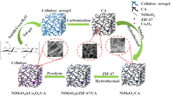
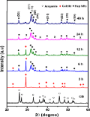
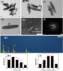
- composite. ZIF-67 is processed into Co3O4 by an annealing process reported previously [32]. The resulting Co3O4 exhibits a nest-like structure and a porous morphology, and the dodecahedral structure is largely kept with no apparent collapse. The TEM image in Figure 2f clearly shows that the Co3O4 particles




Fabrication of Ag-modified hollow titania spheres via controlled silver diffusion in Ag–TiO2 core–shell nanostructures
Beilstein J. Nanotechnol. 2020, 11, 141–146, doi:10.3762/bjnano.11.12

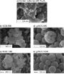
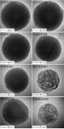
- investigated using SEM and X-ray photoelectron spectroscopy, respectively. The optical properties of the synthesized structures were characterized using UV–vis spectroscopy. Ag–TiO2 hollow nanostructures with different optical properties were prepared simply by a change of the annealing time in the last
- silver diffusion in Ag–TiO2 core–shell nanostructures (CSNs). Our approach comprises three simple steps starting from the synthesis of the metallic core, through its coating with titania and finally annealing leading to plasmonic hollow nanostructures with plasmon resonance in a broad spectral range. SEM
- structures are shown in Figure 1 (down left) and in Figure 2A. Interestingly, further thermal modification of these fabricated Ag@TiO2 CSNs yields unexpected results. Annealing of Ag@TiO2 nanostructures in a muffle furnace results in Ag diffusion from the silver core into the titania shell. As a result, the



Molecular architectonics of DNA for functional nanoarchitectures
Beilstein J. Nanotechnol. 2020, 11, 124–140, doi:10.3762/bjnano.11.11

- structure. In a DNA hybridization process, the oligonucleotides with complementary base sequences are dissolved in a buffer solution and subjected to annealing, which involves a cycle of heating the solution followed by cooling [31]. Seeman and co-workers envisioned the construction of 3D nanoarchitectures
- compared to ssDNA. The selection of the correct base pairing sequence and order enabled the assembly of DNA with balanced rigidity and flexibility within the nanomaterial systems. The maintenance of an exact stoichiometry and long annealing period were the major criteria to achieve defect-free
- inserted into the center of a 13-mer oligonucleotide sequence in an automated DNA synthesizer through phosphoramidite chemistry. The annealing of porphyrin-tethered oligonucleotides with complementary oligonucleotides resulted in the formation of a B-form DNA duplex. The conformational distortion effect


The effect of heat treatment on the morphology and mobility of Au nanoparticles
Beilstein J. Nanotechnol. 2020, 11, 61–67, doi:10.3762/bjnano.11.6

- the geometry from faceted to more rounded shapes were observed with increasing annealing temperature. Kinetic Monte Carlo simulations indicate that the NPs become rounded due to the minimization of the surface area and the transition to lower energy surface types {111} and {100}. The NPs were
- manipulated on a silica substrate with an atomic force microscope (AFM) in tapping mode. Initially, the NPs were immovable by AFM energy dissipation. However, annealed NPs became movable, and less energy was required to displace the NPs annealed at higher temperature. However, after annealing at 800 °C, the
- particles became immovable again. This effect was attributed to the diffusion of Au into the Si substrate and to the growth of the SiO2 layer. Keywords: annealing; atomic force microscopy (AFM); Au nanoparticles; manipulation; melting; nanotribology; Introduction Gold is one of the most prominent


Recent progress in perovskite solar cells: the perovskite layer
Beilstein J. Nanotechnol. 2020, 11, 51–60, doi:10.3762/bjnano.11.5

- -quality perovskite films based on these techniques, researchers control the perovskite morphology by optimizing the solvents for processing [26], varying the annealing temperature [27], adjusting the processing additives [28], sophisticated engineering of the solvent [12][14] and annealing of the solvent


Synthesis of amorphous and graphitized porous nitrogen-doped carbon spheres as oxygen reduction reaction catalysts
Beilstein J. Nanotechnol. 2020, 11, 1–15, doi:10.3762/bjnano.11.1
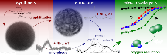
- . Annealing graphene oxide (GO) in an ammonia atmosphere at 550 °C led to pyridinic N-doped graphene, while at a temperature of 850 °C graphitic nitrogen coexisted with pyridinic nitrogen, and for higher temperatures the amount of graphitic N increased. Annealing GO at 850 °C in the presence of polyaniline or
- -carbonized carbon spheres and stirred for 24 h, followed by refluxing for 5 h at 100 °C and subsequent filtration and drying. Catalytic graphitization was carried out by annealing at different temperatures, between 550 and 1000 °C with steps of 150 °C, in argon atmosphere for 4 h (heating rate 5 °C·min−1




Antimony deposition onto Au(111) and insertion of Mg
Beilstein J. Nanotechnol. 2019, 10, 2541–2552, doi:10.3762/bjnano.10.245

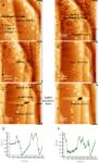
- paper, we will study the kinetics of the insertion process in more detail [19]. Experimental Chemicals, materials and electrolyte The Au(111) single crystal was prepared by cooling down after flame annealing in pure argon (Air Liquid, 99.999%,) atmosphere as described elsewhere [20]. A typical cyclic





Synthesis and acetone sensing properties of ZnFe2O4/rGO gas sensors
Beilstein J. Nanotechnol. 2019, 10, 2516–2526, doi:10.3762/bjnano.10.242
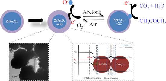
- of ZnFe2O4 and reduced graphene oxide (rGO) with different rGO content were prepared via a simple solvothermal method followed by a high-temperature annealing process in an inert atmosphere. The X-ray diffraction analysis confirmed that the introduction of rGO had no effect on the spinel structure of




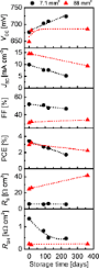
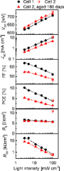
Semitransparent Sb2S3 thin film solar cells by ultrasonic spray pyrolysis for use in solar windows
Beilstein J. Nanotechnol. 2019, 10, 2396–2409, doi:10.3762/bjnano.10.230
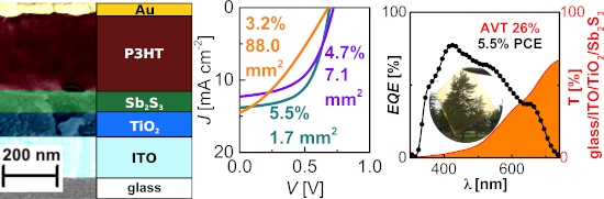
- imposing limitations on the substrate size [43][44]. A recent paper showed a PCE of 4.6% in solar cells based on Sb2(S,Se)3 grown onto planar CdS by USP, followed by Se vapor annealing at ≈400 °C. However, pristine Sb2S3 solar cells consistently yielded a PCE below 0.1% [45]. This clearly illustrates the
- demonstrated that by adapting a two-step sequence, whereby amorphous Sb2S3 layers are first deposited by USP and then crystallized by thermal annealing, compact Sb2S3 thin films with uniform thickness can be fabricated [46]. Similarly, a two-step procedure to grow compact Sb2S3 thin films has become common
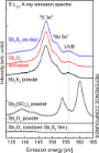
- pattern of the vacuum-annealed sample matched orthorhombic Sb2S3 (ICDD PDF 01-075-4012). The Raman spectrum of the as-deposited Sb2S3 layer contains two broad bands (Figure 1e), which are characteristic of amorphous Sb2S3 [28][46]. After vacuum annealing, characteristic narrower bands of Sb2S3 are



Deterministic placement of ultra-bright near-infrared color centers in arrays of silicon carbide micropillars
Beilstein J. Nanotechnol. 2019, 10, 2383–2395, doi:10.3762/bjnano.10.229
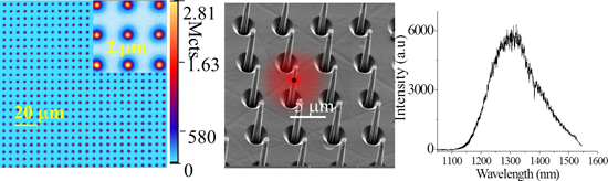
- defects. The maximum H+ concentration was simulated to be at 2 µm under the sample surface. Annealing at different temperatures under neutral N2 atmosphere was used to promote the presence of different defects (VSi without annealing, 750 °C for 30 min for VSiVC, 900 °C for 30 min for NCVSi). The following
- -temperature PL shows an enhancement by a factor of up to 5.5 for VSi in sample 1 and by a factor of 2.3 for VSiVC in sample 3. Our results also confirm the conversion of VSi to VSiVC during annealing [55] from sample 2 to sample 3. The enhancement of VSi in sample 2 appears to be lower than that in sample 1
- after the fabrication of the pillars. For excitation at 940 nm the PL spectra of sample 3 shows the activation of the NCVSi emission at low temperature [35] after annealing at a higher temperature (Figure 3). Only sample 3 at 940 nm excitation is shown here, as it is most exemplary for the formation of


Polyvinylpyrrolidone as additive for perovskite solar cells with water and isopropanol as solvents
Beilstein J. Nanotechnol. 2019, 10, 2374–2382, doi:10.3762/bjnano.10.228

- for 10 min. Then the film was submerged in the MAX solution (the concentration of the MAX solution was 40 mg/mL MAI and 10 mg/mL MACl) for 500 s to prepare the CH3NH3PbI3 layer, and the films were dried by spinning at 3000 rpm for 10 s and annealing at 120 °C for 10 min. Subsequently, the hole
- irradiated by UV/ozone. The following most critical point in the production of the perovskite layer was to spin the lead nitrate onto the SnO2 ETL. Then, the layer was introduced into a bath of MAX solution for 500 s, and finally dried by spinning and annealing at 120 °C for a period of 10 min. The SEM