

Search results
Search for "force" in Full Text gives 1140 result(s) in Beilstein Journal of Nanotechnology. Showing first 200.
Supramolecular one-dimensional conducting nanofibers from a C3-symmetric tetrathiafulvalene derivative
Beilstein J. Nanotechnol. 2026, 17, 872–881, doi:10.3762/bjnano.17.63
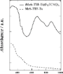
- measurements The structures formed on mica substrates were observed using an atomic force microscopy (AFM) system (Bruker Multi Mode 8). Measurements were performed in non-contact mode using a silicon cantilever with a spring constant of approximately 0.8 N·m−1. Optical spectra UV–vis absorption spectra were
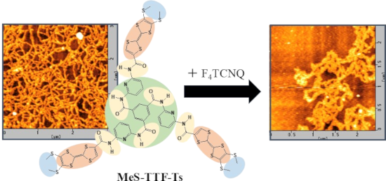
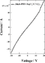
- nanofibers from C3-symmetric MeS-TTF-Ts and the (MeS-TTF-Ts)(F4TCNQ)3 charge-transfer complex In order to form conductive fibers using MeS-TTF-Ts, it was necessary to identify suitable conditions for controlling the formation of supramolecular structures. Atomic force microscopy (AFM) observations of cast


He+ FIBID-fabricated 3D AFM tip architectures: an exploratory study of hollow pillars, helices, and spirals
Beilstein J. Nanotechnol. 2026, 17, 863–871, doi:10.3762/bjnano.17.62
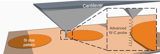
- , Germany 10.3762/bjnano.17.62 Abstract Atomic force microscopy (AFM) relies strongly on tip geometry and mechanical integrity for stable and reproducible surface measurements. Here, we present an exploratory study of tungsten–carbon (W–C) AFM tips with complex three-dimensional (3D) architectures
- required. Keywords: 3D-printed tips; AFM tips; beam induced nanomanufacturing; focused ion beam induced deposition (FIBID); helium ion microscope; nanohelix; nanopillar; nanospiral; scanning tip microscopy; surface topography; tungsten carbide; Introduction The atomic force microscope (AFM) is a
- exhibit high purity [22][23], making them suitable candidates for magnetic force microscopy (MFM) tips [13][14]. However, the magnetic performance of cobalt-based deposits may be affected by oxidation under ambient conditions, as the formation of cobalt oxide can reduce or suppress ferromagnetic behaviour


Light-driven ammonia electrooxidation via carbon nitride–ruthenium molecular interfaces
Beilstein J. Nanotechnol. 2026, 17, 854–862, doi:10.3762/bjnano.17.61
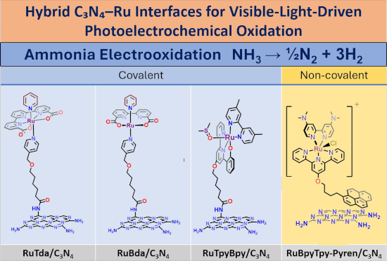
- driving force for many reduction reactions. Its valence band edge at approximately +1.6 V vs NHE supports oxidation chemistry. It is chemically inert to most organic solvents and electrolytes, thermally stable in air up to around 600 °C, and biocompatible. Crucially for hybrid material design, the
- challenge of driving thermodynamically uphill reactions [29][36]. Pure photocatalysis relies entirely on photon energy to supply the thermodynamic driving force, imposing strict requirements on the semiconductor band positions relative to the reaction redox potentials, and offering limited kinetic control


Nanoparticle delivery systems for HIV pre-exposure prophylaxis (PrEP): advances and challenges
Beilstein J. Nanotechnol. 2026, 17, 839–853, doi:10.3762/bjnano.17.60
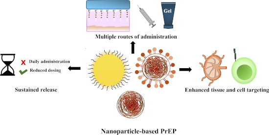
- complementary line of research, hybrid nanocarriers have been developed not just for prophylaxis but for HIV reservoir reactivation or latency reversal. Latency reversal refers to the awakening of dormant HIV to force viral expression within cellular reservoirs, such as resting CD4+ T cells, so that the


Cross-scale design of chemosensor arrays: from molecular self-assembly in water to paper-based devices for metal ion detection
Beilstein J. Nanotechnol. 2026, 17, 828–838, doi:10.3762/bjnano.17.59
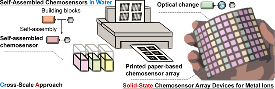
- bond chemistry require organic synthetic approaches in the chemosensor preparations [6][7][8][9]. Meanwhile, molecular self-assembly serves as a driving force for easy-to-obtain chemosensors through spontaneous preparation without a synthetic burden [17]. Moreover, the optical properties of


Sustainable fabrication of 2D-based devices through reuse of substrates with microfabricated electrodes
Beilstein J. Nanotechnol. 2026, 17, 818–827, doi:10.3762/bjnano.17.58
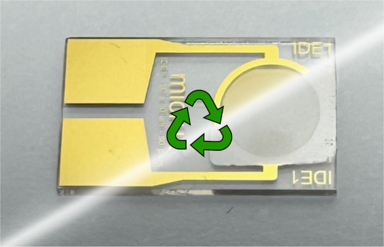
- ), enabling the removal of 2D materials without damaging the electrodes. Electrical measurements, Raman analysis, and Kelvin probe force microscopy measurements collectively confirm the feasibility of repeatedly reusing the same pre-patterned chip, showing that the cleaned regions exhibit no detectable Raman
- interpolation. The Si 520 cm−1 maps in Supporting Information File 1, Figure S9g–i provide additional contrast between the SiO2/Si channel and the Au electrode. In addition, Kelvin probe force microscopy (KPFM) measurements, presented in Supporting Information File 1 (Figures S10 and S11), show that the
- . Kelvin probe force microscopy KPFM measurements were carried out on the same electrode in two states, that is, pristine electrode and electrode after roll-to-roll mechanically exfoliated MoS2 transfer followed by NMP cleaning. Morphology and surface-potential characterization were performed under ambient


Substrate-dependent pore formation in molybdenum disulfide monolayers under ion irradiation
Beilstein J. Nanotechnol. 2026, 17, 769–780, doi:10.3762/bjnano.17.54
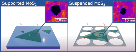
- , high-resolution scanning transmission electron microscopy (STEM) generally requires freestanding membranes, while atomic-resolution atomic force microscopy (AFM) and scanning tunneling microscopy (STM) demand exceptionally clean surfaces; also, substrate effects can further complicate interpretation


Tailoring Ag–Pt nanoalloys through solid-state dewetting: structural and optical insights
Beilstein J. Nanotechnol. 2026, 17, 748–759, doi:10.3762/bjnano.17.52

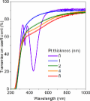
- plasmonic properties. Results and Discussion As-deposited thin Ag–Pt bilayers exhibit a granular morphology, as evidenced by atomic force microscopy (AFM) measurements shown in Figure 1. This granular character leads to instability of the layers at higher temperatures, causing cracking of the continuous




afspm: A framework for manufacturer-agnostic automation in scanning probe microscopy
Beilstein J. Nanotechnol. 2026, 17, 653–667, doi:10.3762/bjnano.17.45
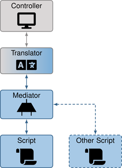
- interfaces types. An automated experiment was run to ensure overall running beyond integration testing. Keywords: atomic force microscopy; automation; manufacturer-agnostic; scanning probe microscopy; software framework; Introduction In scanning probe microscopy (SPM), an atomically sharp tip is scanned
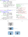
- earlier sample script. In Figure 5, we see pseudocode (Figure 5a) and a system diagram (Figure 5b) for a script including experiment-specific parameters within it. In coupling the algorithmic logic and experiment-specific parameters, we force a new copy of the base script for each new experiment. Imagine
- directly from the computer hard drive, which simplifies the translator logic as it does not need to monitor data live (which is accessible for only some controllers). The exposed level of control assumes the user has pre-configured their “operating mode” (e.g., amplitude-modulated atomic force microscopy




Recent progress in enhancing built-in electric fields of perovskite solar cells via junction engineering
Beilstein J. Nanotechnol. 2026, 17, 602–621, doi:10.3762/bjnano.17.42
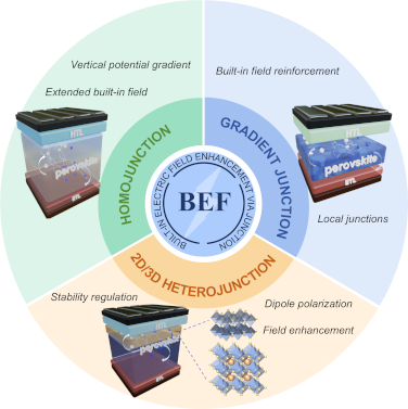
- , carriers migrate at the interface through diffusion and drift, gradually establishing a built-in electric field (BEF) that aligns the Fermi levels on both sides. This field is not only the primary driving force that sustains carrier separation but also a direct determinant of device photovoltaic conversion
- , characterized by band discontinuities or polarization barriers. Its primary role is to modulate the local potential distribution and establish a stable BEF. In materials such as perovskites, which are mixed ionic–electronic conductors, the junction not only determines the driving force for carrier separation
- continuous barrier-reducing channel across the film [15], a strategy that emphasizes longitudinal potential continuity and a “capacitive accumulation” effect, which maintains an effective driving force over a larger thickness and is often accompanied by improved crystallinity and stress release



Probing tribological evolution in atomically thin MoS2 at different scales
Beilstein J. Nanotechnol. 2026, 17, 586–597, doi:10.3762/bjnano.17.40
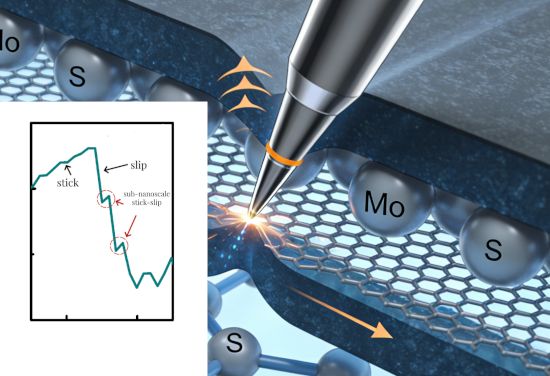
- (MoS2) under controlled loads using a calibrated atomic force microscope (AFM), with a focus on quantifying the strengthening effect and sub-nanoscale stick–slip motion. Our results reveal that the nanoscale strengthening effect intensifies with increasing applied load but weakens as the number of MoS2
- nanoscale to sub-nanoscale, providing critical insights for designing low-friction coatings and high-performance micro/nanoelectromechanical systems (MEMS/NEMS). Keywords: atomic force microscopy; MoS2; strengthening effect; sub-nanoscale stick–slip motion; Introduction Nanoscale friction is a pivotal
- atomic lattice site until the lateral force overcomes interfacial interactions, followed by an instantaneous “slip” to the next stable site [9]. This stick–slip motion is widely regarded as the elementary mechanism of energy dissipation in nanoscale friction, underpinning efforts to understand energy


Defects and defect-mediated engineering of two-dimensional materials: challenges and open questions
Beilstein J. Nanotechnol. 2026, 17, 454–488, doi:10.3762/bjnano.17.31
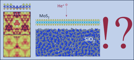
- of defects, for example, TEM [80], STM [81], or atomic force microscopy (AFM) [82]; but, normally, only a small part of the sample can be probed [83][84][85]. Moreover, these techniques can create defects themselves, for example, when the energy of the electron beam exceeds the displacement threshold
- host vacancy clusters. The clusters are also size-limited, as clusters growing too large and into the bright areas would force Gr bonds to detach from the substrate. Therefore, vacancies diffusing around avoid attachment to large clusters and prefer to attach to smaller ones, making the size





Nanocarrier-integrated multilayer films produced by 3D printing for improved skin adhesion and curcumin photostability
Beilstein J. Nanotechnol. 2026, 17, 440–453, doi:10.3762/bjnano.17.30
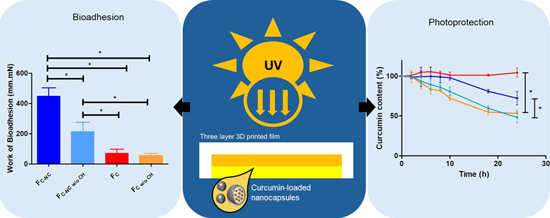
- with absorbent paper. Skin samples were fixed to the equipment probe with instantaneous adhesive, while films were fixed to the equipment’s platform with double-sided tape. The equipment promoted contact between the skin sample and the film, with a force of 290 mN for 3 min. The probe holding the skin
- sample was then withdrawn from the surface of the film by the platform at a constant speed of 0.10 mm/s until total displacement was achieved. The work required to detach the skin sample from the 3D-printed films was calculated based on the peak force and maximum displacement after complete detachment
- requires a minimum applied stress to initiate flow (yield stress), which, in practical terms, corresponds to the force required to extrude the hydrogel through the syringe nozzle during printing. If the applied stress is below the yield stress, the hydrogel remains structurally intact inside the syringe


Ferroelectric nanodot reservoir for neuromorphic computing
Beilstein J. Nanotechnol. 2026, 17, 352–364, doi:10.3762/bjnano.17.24
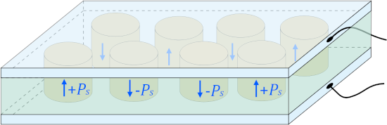
- interfaces. An alternative configuration is shown in Figure 7b, where atomic force microscopy or piezoresponse force microscopy are used for both input and output operations. Here, the localized tip of the microscope is used to inject or sense charges at specific positions in the ferroelectric array
- and readout realized via atomic or piezoresponse force microscopy. Funding This research was funded by the European Union HORIZON action MSCA-SE-3D-TOPO (project number 101236483). A.R. acknowledges the Slovenian Research Agency support (P1-0125). The work of V.V. was supported by Terra Quantum AG.


Calculation of the dynamic stiffness of a cantilever under torsional oscillation
Beilstein J. Nanotechnol. 2026, 17, 303–308, doi:10.3762/bjnano.17.21
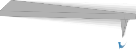
- Keita Nishida Yuuki Yasui Yoshiaki Sugimoto Department of Advanced Materials Science, The University of Tokyo, Chiba 277-8561, Japan 10.3762/bjnano.17.21 Abstract Atomic force microscopy using Si cantilevers provides an effective means for investigating both conservative and dissipative
- : atomic force microscopy; dynamic stiffness; energy dissipation; friction; torsional oscillation mode; Introduction Friction serves as a fundamental mechanism of energy dissipation [1]. While friction typically arises from direct mechanical contact between surfaces, energy dissipation can also occur even
- detailed mechanisms remain not fully understood [5]. Non-contact atomic force microscopy (nc-AFM) is widely employed to investigate non-contact friction through its dissipation channel. Common techniques include pendulum AFM, bimodal AFM, and quartz tuning fork AFM [6][7][8]. Pendulum AFM uses cantilevers

Fast vortex dynamics and relaxation times in NbRe-based heterostructures
Beilstein J. Nanotechnol. 2026, 17, 292–302, doi:10.3762/bjnano.17.20
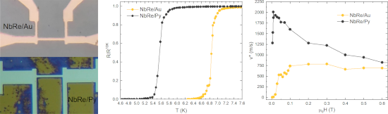
- superconducting gap, Δ(T), quasiparticles diffuse into the surrounding superconducting region, reducing the number of excitations within the core. This process results in a shrinkage of the vortex followed by a decrease of the viscous drag force, fvd, and an increase in the vortex velocity v [9]. When v exceeds
- the critical value v*, the Lorentz force dominates the viscous drag force, leading to instabilities in vortex motion. The dependence of v* on T is given by: where Tc is the superconducting critical temperature, D is the quasiparticles diffusion coefficient, and ζ(x) is the Riemann zeta function. The
- larger experimental Bs measured for the NbRe/Au microbridge thus points to a more efficient edge barrier with respect to the case of NbRe/Py bilayer where the value of Bs is smaller. The latter also exhibits a higher Jc compared to NbRe/Au, indicating a stronger vortex pinning force in this range


Advancing nanolithography: a comprehensive review of materials for local anodic oxidation with AFM
Beilstein J. Nanotechnol. 2026, 17, 275–291, doi:10.3762/bjnano.17.19
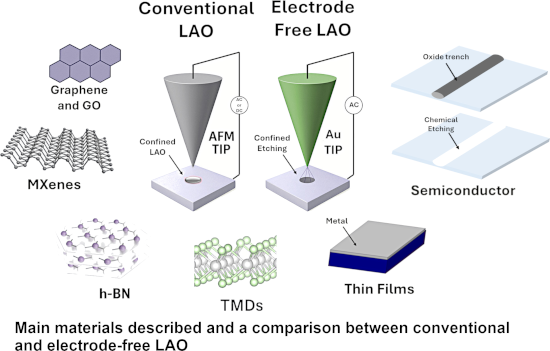
- technique for nanoscale patterning, leveraging the precision of scanning probe microscopy, relying specifically on atomic force microscopy. This review explores the materials utilized in LAO experiments, including semiconductors, metals, insulators, two-dimensional (2D) materials, and emerging
- oxide growth on a silicon surface during LAO, illustrating the formation of a protruding oxide feature and the corresponding buried oxide volume. Reproduced from [8], M. Lorenzoni and F. Pérez-Murano, “Conductive Atomic Force Microscopy for Nanolithography Based on Local Anodic Oxidation,” in Conductive
- Atomic Force Microscopy: Applications in Nanomaterials, with permission from John Wiley and Sons. Copyright © 2017 Wiley-VCH GmbH. This content is not subject to CC BY 4.0. (c) AFM images of square oxide patterns fabricated by LAO on SiC before and after wet etching. (d) Height profile of the top left


Development and in vitro evaluation of liposomes and immunoliposomes containing 5-fluorouracil and R-phycoerythrin as a potential phototheranostic system for colorectal cancer
Beilstein J. Nanotechnol. 2026, 17, 97–121, doi:10.3762/bjnano.17.7
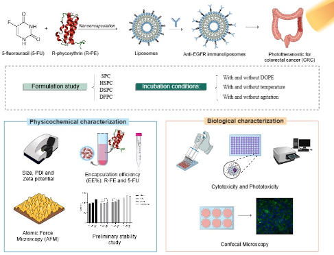
- force microscopy The topographical characterization of liposomal formulations was performed by using atomic force microscopy (AFM) with a Nanosurf® FlexAFM system. The samples analyzed included liposomes and immunoliposomes containing R-PE. Briefly, to avoid vesicle deformation or disruption, liposomes
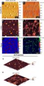
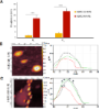
- images were captured using the Nanosurf C3000i software and subsequently processed and analyzed with the Gwyddion v 2.66 software, which was used for image leveling, coloring, 3D visualization of the specimens, and roughness analysis [26]. 2.3.5.1 Atomic force microscopy roughness calculation. Roughness
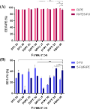
- HSPC IM 07 formulation exhibits the most favorable characteristics for application in delivery systems, balancing nanoscale size, acceptable PDI, and high conjugation efficiency. 3.3 Atomic force microscopy assays Atomic force microscopy assays were used to characterize the surface topography of



Quantitative estimation of nanoparticle/substrate adhesion by atomic force microscopy
Beilstein J. Nanotechnol. 2026, 17, 1–14, doi:10.3762/bjnano.17.1

- of copper nanoparticles to silicon substrates deposited under varying conditions using DC magnetron sputter inert gas condensation. Atomic force microscopy was utilized as a tool for the manipulation of the nanoparticles and to measure lateral forces for their displacement, with cantilever
- calibration achieved through wedge and diamagnetic lateral force calibrator methods. The work of adhesion was quantified by integrating the obtained lateral forces over the distance moved during manipulation, revealing a non-monotonic dependency on nanoparticle size with maximum adhesion observed for
- particles between 6 and 12 nm. In addition, an applied positive substrate bias voltage led to more energetic landing conditions and thus to increased adhesion forces. This study underscores the suitability of atomic force microscopy in characterizing adhesion on the nanoscale and offers insights into future



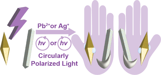
Chiral plasmonic nanostructures fabricated with circularly polarized light
Beilstein J. Nanotechnol. 2025, 16, 2245–2264, doi:10.3762/bjnano.16.154
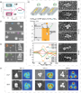
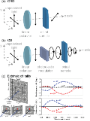
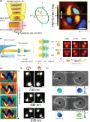
- ”. In the same paper, the authors attributed the formation of chiral AuNPs to the assembly of small NPs under the mechanical force of CPL. The spatial dissymmetry of hot carrier-induced chemical reactions was not discussed. While Figure 4a represents chiral metallic cPNSs synthesized in solution, Figure
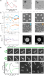
- can lead to a significant displacement of the polymer backbone, with the degree of displacement being dependent on the strength of the electric field under CPL. Chiral topographic changes due to the polymer displacement were observed using atomic force microscopy (AFM). Similar observations were made





Ultrathin water layers on mannosylated gold nanoparticles
Beilstein J. Nanotechnol. 2025, 16, 2183–2198, doi:10.3762/bjnano.16.151
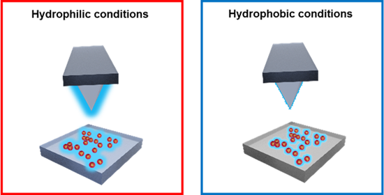
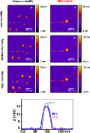
- light scattering, and infrared spectroscopy. We probed particles adsorbed on hydrophilic and hydrophobic surfaces with atomic force microscopy (AFM) and vibrational sum frequency generation (VSFG) spectroscopy, both operated under variable air humidity. For AFM, we additionally tested hydrophilic and
- inorganic surfaces, usually modified with organic layers, and probed by Fourier-transform infrared spectroscopy (FTIR), vibrational sum frequency generation (VSFG), and atomic force microscopy (AFM). For VSFG and AFM, we systematically varied the relative air humidity (RH). DLS and ZP yield particle size
- (Keysight, Scientec, FR), in air in AC “noncontact” mode at 24 °C, at speeds between 0.8 and 1.2 lines/s. The scanning was performed in at least six replicates per condition for the PEG AuNPs and nine replicates for the dimanno-AuNPs. Silicon cantilevers (Multi 75, Budget Sensors) with a force constant k



Electron transport through nanoscale multilayer graphene and hexagonal boron nitride junctions
Beilstein J. Nanotechnol. 2025, 16, 2132–2143, doi:10.3762/bjnano.16.147
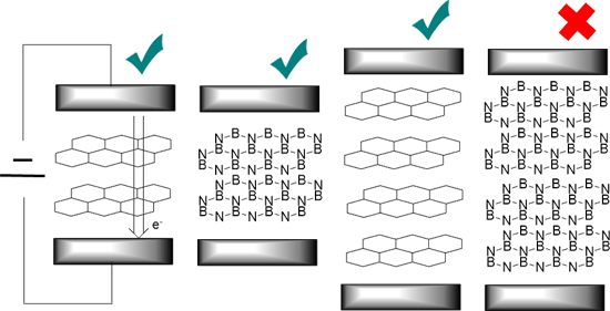
- tunneling behavior. Current–voltage characteristics showed linear dependence at low bias and exponential growth at higher voltages. Conductive atomic force microscopy measurements revealed highly uniform, defect-free tunneling across atomically flat h-BN terraces, with breakdown fields near 1 GV·m−1. These


Rapid synthesis of highly monodisperse AgSbS2 nanocrystals: unveiling multifaceted activities in cancer therapy, antibacterial strategies, and antioxidant defense
Beilstein J. Nanotechnol. 2025, 16, 2105–2115, doi:10.3762/bjnano.16.145
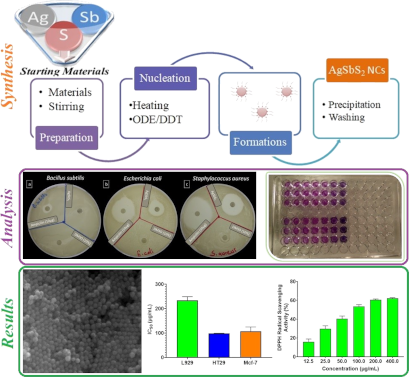
- nanoparticles with bacterial cells and the production of ROS, which causes DNA damage and denaturation of proteins close to the bacterial membrane, causes cell membrane damage [37][38]. In addition, the electrostatic force generated between the bacterial cells and the synthesized NCs causes distraction of the


Toward clinical translation of carbon nanomaterials in anticancer drug delivery: the need for standardisation
Beilstein J. Nanotechnol. 2025, 16, 2092–2104, doi:10.3762/bjnano.16.144
- atomic force microscopy. Surface charge plays a significant role in determining how CNMs interact with biological membranes and intracellular environments. It influences processes such as cellular uptake, cytotoxicity, and inflammatory signalling. For example, BSA-derived negatively charged CDs exhibited




Multifrequency AFM integrating PeakForce tapping and higher eigenmodes for heterogeneous surface characterization
Beilstein J. Nanotechnol. 2025, 16, 2077–2085, doi:10.3762/bjnano.16.142
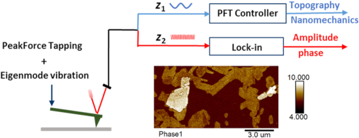
- Yanping Wei Jiafeng Shen Yirong Yao Xuke Li Ming Li Peiling Ke Public Technology Center, Ningbo Institute of Materials Technology and Engineering, Chinese Academy of Sciences, Ningbo 315201, China 10.3762/bjnano.16.142 Abstract This study introduces a multifrequency atomic force microscopy (AFM
- mappings obtained via the PeakForce tapping method. Furthermore, the technique’s dual capability, that is, quantitative mechanics via quasi-static force curves and qualitative material-sensitive information via eigenmode vibration signals, facilitates effective compositional differentiation in
- . Keywords: atomic force microscopy (AFM); high eigenmodes; multifrequency AFM; nanoscale material analysis; surface characterization; Introduction Atomic force microscopy (AFM) has become an indispensable tool for characterizing the morphology and surface properties of materials at the micro- and the