Abstract
High spin polarization and low resistivity of Fe3O4 at room temperature have been an appealing topic in spintronics with various promising applications. High-quality Fe3O4 thin films are a must to achieve the goals. In this report, Fe3O4 films on different substrates (SiO2/Si(100), MgO(100), and MgO/Ta/SiO2/Si(100)) were fabricated at room temperature with radio-frequency (RF) sputtering and annealed at 450 °C for 2 h. The morphological, structural, and magnetic properties of the deposited samples were characterized with atomic force microscopy, X-ray diffractometry, and vibrating sample magnetometry. The polycrystalline Fe3O4 film grown on MgO/Ta/SiO2/Si(100) presented very interesting morphology and structure characteristics. More importantly, changes in grain size and structure due to the effect of the MgO/Ta buffering layers have a strong impact on saturation magnetization and coercivity of Fe3O4 thin films compared to cases of no or just a single buffering layer.
Introduction
Magnetite, also known as Fe3O4, has been extensively researched as one of the most common half-metallic materials in the field of spintronics for a considerable period of time. Magnetoelectronic devices are possible because of the material’s high Curie temperature of 860 K [1], as well as its high spin polarization with only one spin at the Fermi level, even at room temperature [2-6]. Fe3O4 thin films are an issue of interest and have extensive applications in Li-ion batteries, spin Seebeck devices, supercapacitors, spin Hall magnetoresistance, and the study of analog resistive switching of Fe3O4-based cross-cell memristive devices [7-10].
Fe3O4 thin films can be grown by many processes, including molecular beam epitaxy, which is employed for depositing single crystal films, and pulsed laser deposition, which is utilized to achieve epitaxial films [11-13]. The RF magnetron sputtering technique is extensively utilized because of its cost-effectiveness, simplicity, effectiveness, and capacity to produce Fe3O4 films with remarkable uniformity. The qualities of the films can be modified by manipulating parameters throughout the growth process [14,15]. The impact of substrate temperature, annealing temperature, gas flow rate, and thickness on enhancing the characteristics of Fe3O4 thin films has been examined [15-18]. The substrates play a crucial role in directing the growth and enhancing the quality of the crystal, resulting in significant changes in the film’s characteristics [19,20].
Roy et al. conducted a study on polycrystalline Fe3O4 films on Si and SiO2/Si substrates. Their findings revealed that the value of the Gilbert damping parameter is significantly higher in Fe3O4/Si films compared to Fe3O4/SiO2/Si films [21]. Hong and coworkers deposited Fe3O4 films on a MgO substrate, which exhibited a change in the direction of Fe3O4 crystal formation. The directions (222), (400), and (440) of the Fe3O4 peak matched, respectively, the (111), (100), and (110) orientations of the MgO substrate [22]. In addition, Zhang et al. successfully applied a layer of Fe3O4(001) on a MgO(001) substrate. The resulting material exhibited saturation magnetization and magnetic moment values of 407 ± 5 emu/cm3 (3.26 ± 0.04 μB/(f.u.)) and 3.31 ± 0.15 μB/(f.u.), respectively [23].
This paper addresses the deposition of Fe3O4 thin films on three different types of substrates, namely an amorphous SiO2/Si(100) substrate, a single crystal MgO(100) substrate, and a buffer layer consisting of MgO/Ta/SiO2/Si(100). The properties of Fe3O4 thin films were analyzed using atomic force microscopy (AFM), X-ray diffractometry (XRD), and vibrating sample magnetometry (VSM). It is interesting to note that the saturation magnetization of the Fe3O4 films was significantly improved (278.9 emu/cm3) when utilizing a Ta interlayer located between MgO and SiO2, compared to films on SiO2 (136.3 emu/cm3) and MgO(100) (126.3 emu/cm3) substrates. This indicates the potential to facilitate the development of novel magnetic and spintronic architectures.
Results and Discussion
AFM and line-cut method were used to examine the surface morphology and grain sizes of the Fe3O4 films that were formed on SiO2/Si(100), MgO(100), and MgO/Ta/SiO2/Si(100) multilayer substrates (referred to as samples 1, 2, and 3, recpectively). Topography images, with dimensions of 1 × 1 μm2, are shown in Figure 1. They show spherical particles with rather consistent grain sizes. In particular, samples 1 and 2 present grain size values of 7.6 ± 0.5 nm and 9.9 ± 0.6 nm, respectively. Sample 3, grown on the MgO/Ta/SiO2 multilayer structure, reveals the largest value of 31.4 ± 1.4 nm. In addition, the Fe3O4 samples present quite different root-mean-square (RMS) roughness values of 0.94 ± 0.09 nm, 1.29 ± 0.14 nm, and 3.58 ± 0.58 nm for samples 1, 2 and 3, respectively. Sample 3 with the highest value has the roughest surface among the three. These results indicate that the substrate type does have an effect on grain size and roughness of Fe3O4 thin films. Tantalum in the multilayer structure prevents the diffusion of oxygen atoms from SiO2 into MgO leading to enhanced stability of MgO [24,25]. Besides, there was nearly no oxygen diffusion from the Fe3O4 film into the MgO layer, resulting in higher crystallinity and improved grain size as seen in the XRD patterns. Surface properties obtained from Figure 1 are summarized in Table 1.
![[2190-4286-15-101-1]](/bjnano/content/figures/2190-4286-15-101-1.png?scale=2.0&max-width=1024&background=FFFFFF)
Figure 1: AFM images (1 × 1 µm2) of Fe3O4 thin films on different substrates. (a) SiO2, (b) MgO(100), and (c) MgO/Ta/SiO2.
Figure 1: AFM images (1 × 1 µm2) of Fe3O4 thin films on different substrates. (a) SiO2, (b) MgO(100), and (c)...
The crystal structures of the Fe3O4 samples on different substrates were investigated with XRD measurements, and the corresponding diffraction patterns are depicted in Figure 2. The Fe3O4 sample grown on the SiO2/Si(100) substrate exhibits a single Fe3O4(311) peak located at 35.5° (black line), while the one deposited on MgO(100) exhibits the Fe3O4(400) peak at 43.07° (red line). This indicates the epitaxial growth of the Fe3O4 thin film on MgO(100). To our surprise, the Fe3O4 thin film deposited on the multilayer structure shows the two peaks Fe3O4(311) and Fe3O4(400) at 35.68° and 43.36°, respectively (blue line). This implies that the tantalum interlayer has an effect on the crystallization of the Fe3O4 film.
![[2190-4286-15-101-2]](/bjnano/content/figures/2190-4286-15-101-2.png?scale=2.0&max-width=1024&background=FFFFFF)
Figure 2: XRD spectra of sample 1 (black), sample 2 (red), and sample 3 (blue) on SiO2, MgO(100) and MgO/Ta/SiO2, respectively.
Figure 2: XRD spectra of sample 1 (black), sample 2 (red), and sample 3 (blue) on SiO2, MgO(100) and MgO/Ta/S...
XRD patterns provide further information about the structural properties of a material, such as lattice constant (a), dislocation density (δ), and microstrain (ε). Bragg’s law was used to calculate the d-spacing of the Fe3O4(311) and Fe3O4(400) peaks [26,27]:
![[2190-4286-15-101-i1]](/bjnano/content/inline/2190-4286-15-101-i1.svg?max-width=590&scale=1.18182)
where n is the order of diffraction (n = 1) and λ is the X-ray wavelength (Cu Kα, λ = 1.5406 Å). The lattice constant a of the three Fe3O4 samples was determined by [27,28]:
![[2190-4286-15-101-i2]](/bjnano/content/inline/2190-4286-15-101-i2.svg?max-width=590&scale=1.18182)
The microstrain in these samples can be calculated from the lattice constant a above by using the following relation [27,28]:
![[2190-4286-15-101-i3]](/bjnano/content/inline/2190-4286-15-101-i3.svg?max-width=590&scale=1.18182)
where a0 is the lattice parameter of bulk Fe3O4 (a0 = 8.397 Å [29]). Microstrain is a crucial factor that helps to analyze the existence of strain and deformation in thin films [30,31].
The d-spacing values of the Fe3O4(311) and Fe3O4(400) peaks of sample 3 are 2.514 and 2.085 Å, respectively, which are smaller than those on SiO2 (2.527 Å) and MgO(100) (2.099 Å) substrates. These low d-spacing values can be caused by the microstrain in all Fe3O4 samples [27,28]. The Fe3O4 film grown on the multilayer structure is under a higher compressive strain of −0.70% and −0.67%, corresponding to the Fe3O4(311) and Fe3O4(004) peaks, respectively, than samples 1 and 2 with values of −0.19% and −0.01%, respectively. Sample 3 exhibits a decrease in d-spacing for both the (311) and (400) peaks, in comparison to sample 1 and sample 2. The presence of compressive stress in the crystallites of the Fe3O4 thin films causes a shift in the peak observed in sample 3 [32]. Our results reveal that the growth orientation of the Fe3O4 thin film depends on the lattice mismatch between the Fe3O4 thin film and the substrate or buffer layer. When the Fe3O4 thin film is deposited on the amorphous SiO2 substrate, the lattice mismatch between the amorphous substrate and the crystalline film is large. In this case, the growth orientation of Fe3O4 thin film is determined by the direction having the least internal energy, which is [111]. The energetically favored [111] direction also has the highest probability of occupying random dangling bonds from the amorphous substrate surface because it has the highest areal density [13,33]. In contrast, the small lattice mismatch between Fe3O4 thin film and MgO(100) substrate (≈0.3% [29]) results in the growth orientation controlled by the substrate and leads to the appearance of the [100] direction in Fe3O4/MgO. In addition, the Fe3O4(400) and MgO(200) peaks are close because of the similarity in crystalline structure (cubic) and lattice constant (aFe3O4 = 8.397 Å, aMgO = 4.212 Å [29]). The growth orientation of the Fe3O4 thin film in sample 3 is also affected by the internal energy of the [111] direction in addition to effects from the buffer layer. This explains the highest microstrain value in sample 3. The difference in lattice constants between MgO and Ta (cubic, aTa = 3.3058 Å [34]) puts the MgO buffer layer under a higher strain and creates a larger lattice mismatch between the Fe3O4 thin film and the MgO layer compared to the Fe3O4 thin film and MgO substrate.
In addition, the dislocation density was calculated by the following relation [31]:
![[2190-4286-15-101-i4]](/bjnano/content/inline/2190-4286-15-101-i4.svg?max-width=590&scale=1.18182)
where D is the crystallite size, which can be found by using the Scherrer equation. The dislocation density of sample 1 is the highest, 6.6 × 10⁻⁴ nm−2, resulting from oxygen atoms Fe3O4 occupying random dangling bonds of the SiO2 surface [13,33]. In contrast, Fe3O4 thin films deposited on MgO have a low dislocation density of 0.8 × 10⁻⁴ nm−2 for MgO substrate and 1.9 × 10⁻⁴ nm−2 and 0.9 × 10⁻⁴ nm−2 for MgO with Ta buffer layer. The microstructural properties are summarized in Table 2.
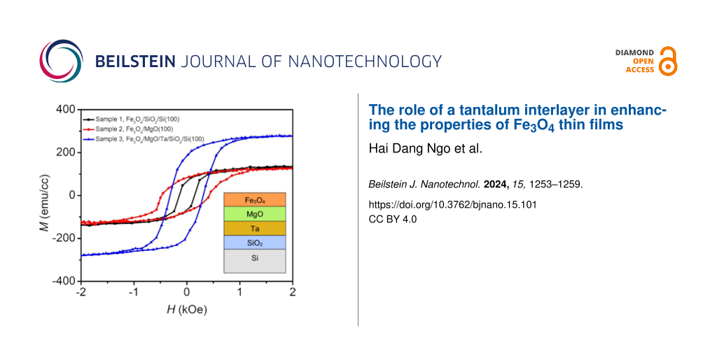
To characterize the effect of microstructure and morphology on the magnetic properties of Fe3O4 thin films, VSM measurements were conducted in an external field from −10 kOe to 10 kOe at room temperature. Figure 3 depicts the hysteresis curves (M–H) of samples 1, 2, and 3. The magnetization of the Fe3O4 thin film grown on the multilayer structure is significantly larger than the those of the others, as shown in Figure 3a. Figure 3b shows a magnification of the M–H loops from −2 kOe to 2 kOe to show more details. The remanent magnetization (Mr) of sample 3 is the largest, 180.9 emu/cm3, while the Mr values of samples 1 and 2 are 66.8 and 84.3 emu/cm3, respectively. All Fe3O4 thin films exhibit saturation at 2 kOe, which is smaller than the values given in other reports [35,36]. The Fe3O4/MgO/Ta/SiO2 sample has a saturation magnetization (Ms) of 278.9 emu/cm3, which is dramatically higher than that of the Fe3O4 thin films on SiO2 (136.3 emu/cm3) and on MgO (126.3 emu/cm3). The coercivity (Hc) of sample 1 is 142.2 Oe, while the Hc values of samples 2 and 3 are 421.2 and 310.1 Oe, respectively. The remanence ratio (Mr/Ms) indicates the amplitude of exchange coupling in Fe3O4 thin films. The results reveal that the remanence ratios of Fe3O4 thin films grown on MgO are larger than that on SiO2. The stronger the exchange coupling, the larger the remanence ratio [37]. The magnetic parameters of the Fe3O4 samples are summarized in Table 3.
![[2190-4286-15-101-3]](/bjnano/content/figures/2190-4286-15-101-3.png?scale=2.0&max-width=1024&background=FFFFFF)
Figure 3: Magnetization of Fe3O4 samples in an external magnetic field in a range of (a) −10 kOe to 10 kOe and (b) −2 kOe to 2 kOe.
Figure 3: Magnetization of Fe3O4 samples in an external magnetic field in a range of (a) −10 kOe to 10 kOe an...
Morphology, microstructure, and anisotropy mechanisms significantly impact the magnetic properties of ferrite materials [38]. It is known that antiphase boundaries (APBs) and grain size in Fe3O4 thin films, which are strongly influenced by substrate or buffer layer, can affect Ms [39,40]. In reports [41,42], APBs in Fe3O4 thin films lead to the reduction of saturation magnetization compared to bulk Fe3O4 (510 emu/cm3) [29]. Therefore, sample 3 has the highest Ms because of the smallest number of APBs among all samples. Using a double buffer layer of MgO/Ta to lower the crystallization temperature can help to reduce the number of APBs in Fe3O4 thin films [43]. Besides, the increased grain size in sample 3 also results in an increased Ms as described in [44]. The change in Hc also depends on two factors, that is, APBs and grain size [45]. Thanks to the prevention of oxygen diffusion of the Ta buffer layer, sample 3 has the largest grain size (Table 1). These large intergranular regions can enhance the number of magnetic moments, making it harder for them to rotate when an external field is applied. Although the grain size in Fe3O4 thin films on the double buffer layer is nearly 3.5 times larger than that in sample 2, the number of APBs in sample 3 is the smallest, resulting in the reduction in Hc of sample 3 compared to the Hc value of sample 2.
Conclusion
Fe3O4 films were prepared on different substrates of SiO2/Si(100), MgO(100), and MgO/Ta/SiO2/Si(100) at room temperature using RF sputtering. Our finding highlights the role of the Ta buffer layer in the multilayered structure. Ta helps to decrease the crystallization temperature of the Fe3O4 film and prevents the diffusion of oxygen atoms from SiO2 to MgO, resulting in an enhancement in grain size and RMS roughness, and in the formation of a polycrystalline structure. Changes in grain size and structure have a strong impact on saturation magnetization and coercivity of the Fe3O4 thin films. Our results indicate that the combination of Ta and MgO buffer layers can influence the morphology and structure of Fe3O4 thin films and help to boost the magnetic properties.
Experimental
RF magnetron sputtering was used at room temperature to grow magnetite films with 40 nm thickness on a variety of substrates, including SiO2, MgO(100), and the multilayer substrate MgO/Ta/SiO2/Si(100). The MgO(100) substrates were prepared by immersing them in a methanol bath at a temperature of 60 °C and drying them in N2 gas flow. Subsequently, the purified substrates were moved into an ultrahigh vacuum (UHV) chamber and underwent a pre-heating process at 600 °C for 30 min in order to eliminate any remaining impurities. The SiO2/Si(100) substrates were immersed in acetone and 2-propanol for a duration of 2 min in an ultrasonic bath. Subsequently, they were immersed in a solution of methanol at a temperature of 60 °C and then dried in N2 gas flow. A 5 nm thick layer of tantalum was deposited on a SiO2/Si(100) substrate using RF magnetron sputtering. This was followed by the formation of a 5 nm thick layer of MgO. The Fe3O4 layers were applied using RF magnetron sputtering at a base pressure of 10−8 Torr, employing a flow of 33 sccm of Ar gas to maintain a stable plasma. The initially deposited films were annealed at a temperature of 723 K for a duration of 2 h under a base pressure of 2.3 × 10⁻⁸ Torr. The Fe3O4 films were analyzed regarding their surface morphology, magnetic properties, and structural properties using atomic force microscopy (EasyScan2, Nanosurf), vibration sample magnetometry (Quantum Design magnetic property measurement system, MPMS-5XL), and X-ray diffractometry (Bruker Discover D8), respectively.
Data Availability Statement
The data that supports the findings of this study is available from the corresponding author upon reasonable request.
References
-
Fonin, M.; Dedkov, Y. S.; Pentcheva, R.; Rüdiger, U.; Güntherodt, G. J. Phys.: Condens. Matter 2007, 19, 315217. doi:10.1088/0953-8984/19/31/315217
Return to citation in text: [1] -
Jain, S.; Adeyeye, A. O.; Boothroyd, C. B. J. Appl. Phys. 2005, 97, 093713. doi:10.1063/1.1889247
Return to citation in text: [1] -
Ding, S.; Tian, Y.; Liu, X.; Zou, Y.; Dong, H.; Mi, W.; Hu, W. Nano Res. 2021, 14, 304–310. doi:10.1007/s12274-020-3089-x
Return to citation in text: [1] -
Hihath, S.; Kiehl, R. A.; van Benthem, K. J. Appl. Phys. 2014, 116, 084306. doi:10.1063/1.4893958
Return to citation in text: [1] -
Wolf, S. A.; Awschalom, D. D.; Buhrman, R. A.; Daughton, J. M.; von Molnár, S.; Roukes, M. L.; Chtchelkanova, A. Y.; Treger, D. M. Science 2001, 294, 1488–1495. doi:10.1126/science.1065389
Return to citation in text: [1] -
Wu, P.-C.; Chen, P.-F.; Do, T. H.; Hsieh, Y.-H.; Ma, C.-H.; Ha, T. D.; Wu, K.-H.; Wang, Y.-J.; Li, H.-B.; Chen, Y.-C.; Juang, J.-Y.; Yu, P.; Eng, L. M.; Chang, C.-F.; Chiu, P.-W.; Tjeng, L. H.; Chu, Y.-H. ACS Appl. Mater. Interfaces 2016, 8, 33794–33801. doi:10.1021/acsami.6b11610
Return to citation in text: [1] -
Wang, X.; Liao, Y.; Zhang, D.; Wen, T.; Zhong, Z. J. Mater. Sci. Technol. 2018, 34, 1259–1272. doi:10.1016/j.jmst.2018.01.011
Return to citation in text: [1] -
Jiang, K.; Sun, B.; Yao, M.; Wang, N.; Hu, W.; Komarneni, S. Microporous Mesoporous Mater. 2018, 265, 189–194. doi:10.1016/j.micromeso.2018.02.015
Return to citation in text: [1] -
Venkat, G.; Cox, C. D. W.; Voneshen, D.; Caruana, A. J.; Piovano, A.; Cropper, M. D.; Morrison, K. Phys. Rev. Mater. 2020, 4, 075402. doi:10.1103/physrevmaterials.4.075402
Return to citation in text: [1] -
Pham, T. K. H.; Ribeiro, M.; Park, J. H.; Lee, N. J.; Kang, K. H.; Park, E.; Nguyen, V. Q.; Michel, A.; Yoon, C. S.; Cho, S.; Kim, T. H. Sci. Rep. 2018, 8, 13907. doi:10.1038/s41598-018-31915-3
Return to citation in text: [1] -
Cao, L.; Guo, Q.; Liang, J.; Kou, Z.; Zhou, X.; Huang, Z.; Zhai, Y.; Du, J.; You, B.; Zhao, H.; Li, Q.; Zhang, W.; Wee, A. T. S.; Wong, P. K. J.; Yu, X. J. Mater. Sci.: Mater. Electron. 2021, 32, 23645–23653. doi:10.1007/s10854-021-06858-7
Return to citation in text: [1] -
Arora, S. K.; Sofin, R. G. S.; Shvets, I. V.; Luysberg, M. J. Appl. Phys. 2006, 100, 073908. doi:10.1063/1.2349468
Return to citation in text: [1] -
Tiwari, S.; Prakash, R.; Choudhary, R. J.; Phase, D. M. J. Phys. D: Appl. Phys. 2007, 40, 4943–4947. doi:10.1088/0022-3727/40/16/028
Return to citation in text: [1] [2] [3] -
Abdulkareem, K. A.; Kadhim, S. M.; Ali, S. B. Eng. Technol. J. 2022, 40, 334–342. doi:10.30684/etj.v40i2.2235
Return to citation in text: [1] -
Sun, L.; Ban, D.; Liu, E.; Li, X.; Peng, H.; Yao, Z.; Huang, Z.; Zhai, Y.; Zhai, H. Thin Solid Films 2020, 693, 137698. doi:10.1016/j.tsf.2019.137698
Return to citation in text: [1] [2] -
Pan, L.; Zhang, G.; Fan, C.; Qiu, H.; Wu, P.; Wang, F.; Zhang, Y. Thin Solid Films 2005, 473, 63–67. doi:10.1016/j.tsf.2004.07.008
Return to citation in text: [1] -
Truong, V. D. T.; Le, T. T. A.; Nguyen, H. N.; Huynh, H. T.; Pham, T. K. H. J. Tech. Educ. Sci. 2022, 17, 34–38. doi:10.54644/jte.72a.2022.1237
Return to citation in text: [1] -
Shameem, P. V. M.; Kumar, M. S. J. Magn. Magn. Mater. 2018, 458, 241–252. doi:10.1016/j.jmmm.2018.03.027
Return to citation in text: [1] -
Tiwari, S.; Choudhary, R. J.; Prakash, R.; Phase, D. M. J. Phys.: Condens. Matter 2007, 19, 176002. doi:10.1088/0953-8984/19/17/176002
Return to citation in text: [1] -
Reisinger, D.; Majewski, P.; Opel, M.; Alff, L.; Gross, R. Appl. Phys. Lett. 2004, 85, 4980–4982. doi:10.1063/1.1808497
Return to citation in text: [1] -
Roy, J.; Teja, P. R.; Sahu, S.; Ali, A.; Basheed, G. A.; Gangineni, R. B. Phys. B (Amsterdam, Neth.) 2024, 687, 416101. doi:10.1016/j.physb.2024.416101
Return to citation in text: [1] -
Hong, X.; Yang, Y.; Xiao, W.; Yang, Y.; Chen, J.; Ding, J. Adv. Electron. Mater. 2015, 1, 1500102. doi:10.1002/aelm.201500102
Return to citation in text: [1] -
Zhang, Z.; Lu, X.; Yan, Y.; Lu, J.; Li, Z.; Liu, Q.; Zhu, F.; Cao, J.; Wang, Y.; Huang, Z.; Zhai, Y.; Li, Y.; Ruan, X.; He, L.; Wu, J.; Du, J.; Zhang, R.; Xu, Y. Appl. Phys. Lett. 2022, 120. doi:10.1063/5.0091241
Return to citation in text: [1] -
Watanabe, K.; Fukami, S.; Sato, H.; Ikeda, S.; Matsukura, F.; Ohno, H. Jpn. J. Appl. Phys. 2017, 56, 0802B2. doi:10.7567/jjap.56.0802b2
Return to citation in text: [1] -
Xue, F.; Sato, N.; Bi, C.; Hu, J.; He, J.; Wang, S. X. APL Mater. 2019, 7, 101112. doi:10.1063/1.5101002
Return to citation in text: [1] -
Alford, T. L.; Feldman, L. C.; Mayer, J. W. Fundamentals of Nanoscale Film Analysis; Springer Science & Business Media: New York, NY, USA, 2007. doi:10.1007/978-0-387-29261-8
Return to citation in text: [1] -
Cullity, B. D. Elements of X-Ray Diffraction; Addison-Wesley Publishing: Reading, MA, USA, 1956.
Return to citation in text: [1] [2] [3] [4] -
Mattox, D. M. Handbook of Physical Vapor Deposition (PVD) Processing, 2nd ed.; William Andrew: Oxford, UK, 2010. doi:10.1016/c2009-0-18800-1
Return to citation in text: [1] [2] [3] -
Nagahama, T.; Matsuda, Y.; Tate, K.; Kawai, T.; Takahashi, N.; Hiratani, S.; Watanabe, Y.; Yanase, T.; Shimada, T. Appl. Phys. Lett. 2014, 105, 102410. doi:10.1063/1.4894575
Return to citation in text: [1] [2] [3] [4] -
Goyal, R. N.; Kaur, D.; Pandey, A. K. J. Nanosci. Nanotechnol. 2010, 10, 8018–8025. doi:10.1166/jnn.2010.3004
Return to citation in text: [1] -
Kurtaran, S. Opt. Mater. (Amsterdam, Neth.) 2021, 114, 110908. doi:10.1016/j.optmat.2021.110908
Return to citation in text: [1] [2] -
Langlet, M.; Joubert, J. C. J. Appl. Phys. 1988, 64, 780–786. doi:10.1063/1.341924
Return to citation in text: [1] -
Huang, X.; Ding, J. J. Korean Phys. Soc. 2013, 62, 2228–2232. doi:10.3938/jkps.62.2228
Return to citation in text: [1] [2] -
Hallmann, L.; Ulmer, P. Appl. Surf. Sci. 2013, 282, 1–6. doi:10.1016/j.apsusc.2013.04.032
Return to citation in text: [1] -
Chen, Y. Z.; Sun, J. R.; Han, Y. N.; Xie, X. Y.; Shen, J.; Rong, C. B.; He, S. L.; Shen, B. G. J. Appl. Phys. 2008, 103, 07D703. doi:10.1063/1.2832305
Return to citation in text: [1] -
Yin, J.-X.; Liu, Z.-G.; Wu, S.-F.; Wang, W.-H.; Kong, W.-D.; Richard, P.; Yan, L.; Ding, H. AIP Adv. 2016, 6, 065111. doi:10.1063/1.4954035
Return to citation in text: [1] -
He, L.; Jiang, Q.; Rehman, S. U.; Song, J.; Ouyang, H.; Zhong, Z. Mater. Res. Express 2019, 6, 096111. doi:10.1088/2053-1591/ab2fb5
Return to citation in text: [1] -
Kotnala, R. K.; Shah, J. Ferrite Materials: Nano to Spintronics Regime. Handbook of magnetic materials; North-Holland: Amsterdam, Netherlands, 2015; Vol. 23, pp 291–379. doi:10.1016/b978-0-444-63528-0.00004-8
Return to citation in text: [1] -
Ramos, A. V.; Moussy, J.-B.; Guittet, M.-J.; Bataille, A. M.; Gautier-Soyer, M.; Viret, M.; Gatel, C.; Bayle-Guillemaud, P.; Snoeck, E. J. Appl. Phys. 2006, 100, 103902. doi:10.1063/1.2386927
Return to citation in text: [1] -
Liu, H.; Jiang, E. Y.; Bai, H. L.; Zheng, R. K.; Zhang, X. X. J. Phys. D: Appl. Phys. 2003, 36, 2950–2953. doi:10.1088/0022-3727/36/23/013
Return to citation in text: [1] -
Singh, S. K.; Husain, S.; Kumar, A.; Chaudhary, S. J. Magn. Magn. Mater. 2018, 448, 303–309. doi:10.1016/j.jmmm.2017.07.082
Return to citation in text: [1] -
Moreno, R.; Jenkins, S.; Skeparovski, A.; Nedelkoski, Z.; Gerber, A.; Lazarov, V. K.; Evans, R. F. L. J. Phys.: Condens. Matter 2021, 33, 175802. doi:10.1088/1361-648x/abe26c
Return to citation in text: [1] -
Pham, T. K. H.; Truong, V. D. T.; Le, V.-Q. J. Ceram. Soc. Jpn. 2022, 130, 948–951. doi:10.2109/jcersj2.22099
Return to citation in text: [1] -
Jafari, A.; Shayesteh, S. F.; Salouti, M.; Boustani, K. J. Magn. Magn. Mater. 2015, 379, 305–312. doi:10.1016/j.jmmm.2014.12.050
Return to citation in text: [1] -
Bollero, A.; Ziese, M.; Höhne, R.; Semmelhack, H. C.; Köhler, U.; Setzer, A.; Esquinazi, P. J. Magn. Magn. Mater. 2005, 285, 279–289. doi:10.1016/j.jmmm.2004.08.004
Return to citation in text: [1]
| 39. | Ramos, A. V.; Moussy, J.-B.; Guittet, M.-J.; Bataille, A. M.; Gautier-Soyer, M.; Viret, M.; Gatel, C.; Bayle-Guillemaud, P.; Snoeck, E. J. Appl. Phys. 2006, 100, 103902. doi:10.1063/1.2386927 |
| 40. | Liu, H.; Jiang, E. Y.; Bai, H. L.; Zheng, R. K.; Zhang, X. X. J. Phys. D: Appl. Phys. 2003, 36, 2950–2953. doi:10.1088/0022-3727/36/23/013 |
| 41. | Singh, S. K.; Husain, S.; Kumar, A.; Chaudhary, S. J. Magn. Magn. Mater. 2018, 448, 303–309. doi:10.1016/j.jmmm.2017.07.082 |
| 42. | Moreno, R.; Jenkins, S.; Skeparovski, A.; Nedelkoski, Z.; Gerber, A.; Lazarov, V. K.; Evans, R. F. L. J. Phys.: Condens. Matter 2021, 33, 175802. doi:10.1088/1361-648x/abe26c |
| 29. | Nagahama, T.; Matsuda, Y.; Tate, K.; Kawai, T.; Takahashi, N.; Hiratani, S.; Watanabe, Y.; Yanase, T.; Shimada, T. Appl. Phys. Lett. 2014, 105, 102410. doi:10.1063/1.4894575 |
| 1. | Fonin, M.; Dedkov, Y. S.; Pentcheva, R.; Rüdiger, U.; Güntherodt, G. J. Phys.: Condens. Matter 2007, 19, 315217. doi:10.1088/0953-8984/19/31/315217 |
| 14. | Abdulkareem, K. A.; Kadhim, S. M.; Ali, S. B. Eng. Technol. J. 2022, 40, 334–342. doi:10.30684/etj.v40i2.2235 |
| 15. | Sun, L.; Ban, D.; Liu, E.; Li, X.; Peng, H.; Yao, Z.; Huang, Z.; Zhai, Y.; Zhai, H. Thin Solid Films 2020, 693, 137698. doi:10.1016/j.tsf.2019.137698 |
| 29. | Nagahama, T.; Matsuda, Y.; Tate, K.; Kawai, T.; Takahashi, N.; Hiratani, S.; Watanabe, Y.; Yanase, T.; Shimada, T. Appl. Phys. Lett. 2014, 105, 102410. doi:10.1063/1.4894575 |
| 11. | Cao, L.; Guo, Q.; Liang, J.; Kou, Z.; Zhou, X.; Huang, Z.; Zhai, Y.; Du, J.; You, B.; Zhao, H.; Li, Q.; Zhang, W.; Wee, A. T. S.; Wong, P. K. J.; Yu, X. J. Mater. Sci.: Mater. Electron. 2021, 32, 23645–23653. doi:10.1007/s10854-021-06858-7 |
| 12. | Arora, S. K.; Sofin, R. G. S.; Shvets, I. V.; Luysberg, M. J. Appl. Phys. 2006, 100, 073908. doi:10.1063/1.2349468 |
| 13. | Tiwari, S.; Prakash, R.; Choudhary, R. J.; Phase, D. M. J. Phys. D: Appl. Phys. 2007, 40, 4943–4947. doi:10.1088/0022-3727/40/16/028 |
| 30. | Goyal, R. N.; Kaur, D.; Pandey, A. K. J. Nanosci. Nanotechnol. 2010, 10, 8018–8025. doi:10.1166/jnn.2010.3004 |
| 31. | Kurtaran, S. Opt. Mater. (Amsterdam, Neth.) 2021, 114, 110908. doi:10.1016/j.optmat.2021.110908 |
| 7. | Wang, X.; Liao, Y.; Zhang, D.; Wen, T.; Zhong, Z. J. Mater. Sci. Technol. 2018, 34, 1259–1272. doi:10.1016/j.jmst.2018.01.011 |
| 8. | Jiang, K.; Sun, B.; Yao, M.; Wang, N.; Hu, W.; Komarneni, S. Microporous Mesoporous Mater. 2018, 265, 189–194. doi:10.1016/j.micromeso.2018.02.015 |
| 9. | Venkat, G.; Cox, C. D. W.; Voneshen, D.; Caruana, A. J.; Piovano, A.; Cropper, M. D.; Morrison, K. Phys. Rev. Mater. 2020, 4, 075402. doi:10.1103/physrevmaterials.4.075402 |
| 10. | Pham, T. K. H.; Ribeiro, M.; Park, J. H.; Lee, N. J.; Kang, K. H.; Park, E.; Nguyen, V. Q.; Michel, A.; Yoon, C. S.; Cho, S.; Kim, T. H. Sci. Rep. 2018, 8, 13907. doi:10.1038/s41598-018-31915-3 |
| 27. | Cullity, B. D. Elements of X-Ray Diffraction; Addison-Wesley Publishing: Reading, MA, USA, 1956. |
| 28. | Mattox, D. M. Handbook of Physical Vapor Deposition (PVD) Processing, 2nd ed.; William Andrew: Oxford, UK, 2010. doi:10.1016/c2009-0-18800-1 |
| 2. | Jain, S.; Adeyeye, A. O.; Boothroyd, C. B. J. Appl. Phys. 2005, 97, 093713. doi:10.1063/1.1889247 |
| 3. | Ding, S.; Tian, Y.; Liu, X.; Zou, Y.; Dong, H.; Mi, W.; Hu, W. Nano Res. 2021, 14, 304–310. doi:10.1007/s12274-020-3089-x |
| 4. | Hihath, S.; Kiehl, R. A.; van Benthem, K. J. Appl. Phys. 2014, 116, 084306. doi:10.1063/1.4893958 |
| 5. | Wolf, S. A.; Awschalom, D. D.; Buhrman, R. A.; Daughton, J. M.; von Molnár, S.; Roukes, M. L.; Chtchelkanova, A. Y.; Treger, D. M. Science 2001, 294, 1488–1495. doi:10.1126/science.1065389 |
| 6. | Wu, P.-C.; Chen, P.-F.; Do, T. H.; Hsieh, Y.-H.; Ma, C.-H.; Ha, T. D.; Wu, K.-H.; Wang, Y.-J.; Li, H.-B.; Chen, Y.-C.; Juang, J.-Y.; Yu, P.; Eng, L. M.; Chang, C.-F.; Chiu, P.-W.; Tjeng, L. H.; Chu, Y.-H. ACS Appl. Mater. Interfaces 2016, 8, 33794–33801. doi:10.1021/acsami.6b11610 |
| 27. | Cullity, B. D. Elements of X-Ray Diffraction; Addison-Wesley Publishing: Reading, MA, USA, 1956. |
| 28. | Mattox, D. M. Handbook of Physical Vapor Deposition (PVD) Processing, 2nd ed.; William Andrew: Oxford, UK, 2010. doi:10.1016/c2009-0-18800-1 |
| 22. | Hong, X.; Yang, Y.; Xiao, W.; Yang, Y.; Chen, J.; Ding, J. Adv. Electron. Mater. 2015, 1, 1500102. doi:10.1002/aelm.201500102 |
| 24. | Watanabe, K.; Fukami, S.; Sato, H.; Ikeda, S.; Matsukura, F.; Ohno, H. Jpn. J. Appl. Phys. 2017, 56, 0802B2. doi:10.7567/jjap.56.0802b2 |
| 25. | Xue, F.; Sato, N.; Bi, C.; Hu, J.; He, J.; Wang, S. X. APL Mater. 2019, 7, 101112. doi:10.1063/1.5101002 |
| 45. | Bollero, A.; Ziese, M.; Höhne, R.; Semmelhack, H. C.; Köhler, U.; Setzer, A.; Esquinazi, P. J. Magn. Magn. Mater. 2005, 285, 279–289. doi:10.1016/j.jmmm.2004.08.004 |
| 21. | Roy, J.; Teja, P. R.; Sahu, S.; Ali, A.; Basheed, G. A.; Gangineni, R. B. Phys. B (Amsterdam, Neth.) 2024, 687, 416101. doi:10.1016/j.physb.2024.416101 |
| 26. | Alford, T. L.; Feldman, L. C.; Mayer, J. W. Fundamentals of Nanoscale Film Analysis; Springer Science & Business Media: New York, NY, USA, 2007. doi:10.1007/978-0-387-29261-8 |
| 27. | Cullity, B. D. Elements of X-Ray Diffraction; Addison-Wesley Publishing: Reading, MA, USA, 1956. |
| 19. | Tiwari, S.; Choudhary, R. J.; Prakash, R.; Phase, D. M. J. Phys.: Condens. Matter 2007, 19, 176002. doi:10.1088/0953-8984/19/17/176002 |
| 20. | Reisinger, D.; Majewski, P.; Opel, M.; Alff, L.; Gross, R. Appl. Phys. Lett. 2004, 85, 4980–4982. doi:10.1063/1.1808497 |
| 43. | Pham, T. K. H.; Truong, V. D. T.; Le, V.-Q. J. Ceram. Soc. Jpn. 2022, 130, 948–951. doi:10.2109/jcersj2.22099 |
| 15. | Sun, L.; Ban, D.; Liu, E.; Li, X.; Peng, H.; Yao, Z.; Huang, Z.; Zhai, Y.; Zhai, H. Thin Solid Films 2020, 693, 137698. doi:10.1016/j.tsf.2019.137698 |
| 16. | Pan, L.; Zhang, G.; Fan, C.; Qiu, H.; Wu, P.; Wang, F.; Zhang, Y. Thin Solid Films 2005, 473, 63–67. doi:10.1016/j.tsf.2004.07.008 |
| 17. | Truong, V. D. T.; Le, T. T. A.; Nguyen, H. N.; Huynh, H. T.; Pham, T. K. H. J. Tech. Educ. Sci. 2022, 17, 34–38. doi:10.54644/jte.72a.2022.1237 |
| 18. | Shameem, P. V. M.; Kumar, M. S. J. Magn. Magn. Mater. 2018, 458, 241–252. doi:10.1016/j.jmmm.2018.03.027 |
| 23. | Zhang, Z.; Lu, X.; Yan, Y.; Lu, J.; Li, Z.; Liu, Q.; Zhu, F.; Cao, J.; Wang, Y.; Huang, Z.; Zhai, Y.; Li, Y.; Ruan, X.; He, L.; Wu, J.; Du, J.; Zhang, R.; Xu, Y. Appl. Phys. Lett. 2022, 120. doi:10.1063/5.0091241 |
| 44. | Jafari, A.; Shayesteh, S. F.; Salouti, M.; Boustani, K. J. Magn. Magn. Mater. 2015, 379, 305–312. doi:10.1016/j.jmmm.2014.12.050 |
| 13. | Tiwari, S.; Prakash, R.; Choudhary, R. J.; Phase, D. M. J. Phys. D: Appl. Phys. 2007, 40, 4943–4947. doi:10.1088/0022-3727/40/16/028 |
| 33. | Huang, X.; Ding, J. J. Korean Phys. Soc. 2013, 62, 2228–2232. doi:10.3938/jkps.62.2228 |
| 27. | Cullity, B. D. Elements of X-Ray Diffraction; Addison-Wesley Publishing: Reading, MA, USA, 1956. |
| 28. | Mattox, D. M. Handbook of Physical Vapor Deposition (PVD) Processing, 2nd ed.; William Andrew: Oxford, UK, 2010. doi:10.1016/c2009-0-18800-1 |
| 32. | Langlet, M.; Joubert, J. C. J. Appl. Phys. 1988, 64, 780–786. doi:10.1063/1.341924 |
| 37. | He, L.; Jiang, Q.; Rehman, S. U.; Song, J.; Ouyang, H.; Zhong, Z. Mater. Res. Express 2019, 6, 096111. doi:10.1088/2053-1591/ab2fb5 |
| 38. | Kotnala, R. K.; Shah, J. Ferrite Materials: Nano to Spintronics Regime. Handbook of magnetic materials; North-Holland: Amsterdam, Netherlands, 2015; Vol. 23, pp 291–379. doi:10.1016/b978-0-444-63528-0.00004-8 |
| 13. | Tiwari, S.; Prakash, R.; Choudhary, R. J.; Phase, D. M. J. Phys. D: Appl. Phys. 2007, 40, 4943–4947. doi:10.1088/0022-3727/40/16/028 |
| 33. | Huang, X.; Ding, J. J. Korean Phys. Soc. 2013, 62, 2228–2232. doi:10.3938/jkps.62.2228 |
| 35. | Chen, Y. Z.; Sun, J. R.; Han, Y. N.; Xie, X. Y.; Shen, J.; Rong, C. B.; He, S. L.; Shen, B. G. J. Appl. Phys. 2008, 103, 07D703. doi:10.1063/1.2832305 |
| 36. | Yin, J.-X.; Liu, Z.-G.; Wu, S.-F.; Wang, W.-H.; Kong, W.-D.; Richard, P.; Yan, L.; Ding, H. AIP Adv. 2016, 6, 065111. doi:10.1063/1.4954035 |
| 34. | Hallmann, L.; Ulmer, P. Appl. Surf. Sci. 2013, 282, 1–6. doi:10.1016/j.apsusc.2013.04.032 |
| 31. | Kurtaran, S. Opt. Mater. (Amsterdam, Neth.) 2021, 114, 110908. doi:10.1016/j.optmat.2021.110908 |
| 29. | Nagahama, T.; Matsuda, Y.; Tate, K.; Kawai, T.; Takahashi, N.; Hiratani, S.; Watanabe, Y.; Yanase, T.; Shimada, T. Appl. Phys. Lett. 2014, 105, 102410. doi:10.1063/1.4894575 |
| 29. | Nagahama, T.; Matsuda, Y.; Tate, K.; Kawai, T.; Takahashi, N.; Hiratani, S.; Watanabe, Y.; Yanase, T.; Shimada, T. Appl. Phys. Lett. 2014, 105, 102410. doi:10.1063/1.4894575 |
© 2024 Ngo et al.; licensee Beilstein-Institut.
This is an open access article licensed under the terms of the Beilstein-Institut Open Access License Agreement (https://www.beilstein-journals.org/bjnano/terms), which is identical to the Creative Commons Attribution 4.0 International License (https://creativecommons.org/licenses/by/4.0). The reuse of material under this license requires that the author(s), source and license are credited. Third-party material in this article could be subject to other licenses (typically indicated in the credit line), and in this case, users are required to obtain permission from the license holder to reuse the material.