

Search results
Search for "resolution" in Full Text gives 1331 result(s) in Beilstein Journal of Nanotechnology. Showing first 200.
Facile synthesis of platinated DNA nanoparticles with radiosensitizing potential
Beilstein J. Nanotechnol. 2026, 17, 1117–1127, doi:10.3762/bjnano.17.76
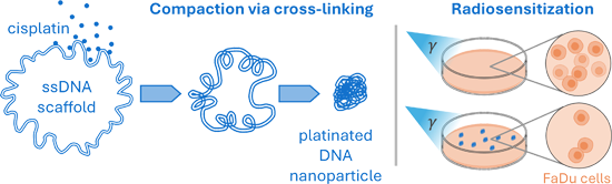
- generated to verify that all particles had been correctly detected. This procedure produced a table containing the projected area of each particle, calibrated in square nanometers according to the image resolution. The equivalent particle diameters were then estimated from the measured projected areas by
- in the particle detection method and image resolution, which cannot fully resolve the “free”, extended portions of the ssDNA scaffold. As a result, only the condensed looped regions are detected as discrete particles. At a 4000 cisplatin/DNA scaffold ratio, however, these localized loops already
- shift may reflect either limitations in AFM resolution at smaller particle sizes or the onset of partial structural degradation. Consistent with this observation, AGE analysis shows a slight mobility shift for samples heated to 90 °C, suggesting minor structural changes at this temperature (Figure 4B


Electrochemical sensing of sildenafil in pharmaceutical formulations using an (S,N)-doped reduced graphene oxide-modified electrode
Beilstein J. Nanotechnol. 2026, 17, 1087–1102, doi:10.3762/bjnano.17.74
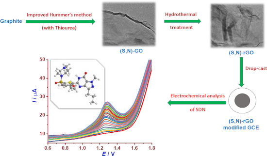
- Quoc Viet, Cau Giay, Hanoi City, 100000, Vietnam 10.3762/bjnano.17.74 Abstract In this work, (S,N)-co-doped reduced graphene oxide ((S,N)-rGO) was successfully synthesized via thermal treatment and thoroughly characterized by X-ray diffraction, high-resolution transmission electron microscopy
- , FTIR, BET, and Raman analyses. High-resolution transmission electron microscopy (HRTEM) images of (S,N)-GO and (S,N)-rGO are presented in Figure 2a and Figure 2b, respectively. The (S,N)-GO sample exhibits thin, transparent, and relatively smooth layered nanosheets with a typical wrinkled morphology



Nanoglasses: a trail towards uncharted regions of vitreous materials and their properties?
Beilstein J. Nanotechnol. 2026, 17, 1047–1062, doi:10.3762/bjnano.17.72
- characteristics. A higher-resolution view is provided by TEM (Figure 3b), which reveals the nanostructured nature of the film. This structure comprises glass grains interspersed with channels, corresponding to glass–glass interfaces. An inset in the bottom right of Figure 3b emphasizes these different regions


Influence of an external electric field on the catalytic CO oxidation of nanoscaled CeO2 and its La3+ and Gd3+ congeners
Beilstein J. Nanotechnol. 2026, 17, 1028–1038, doi:10.3762/bjnano.17.70
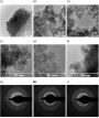
- high-resolution transmission electron microscopy (HRTEM) reveal highly crystalline spherical, slightly faceted nCeO2 and 5% doped-nCeO2 with a diameter of around 15 nm (Figure 1a–c). The observed d-spacings are characteristic of nCeO2 (0.31 nm), Gd3+–nCeO2 (0.31 nm), and La3+–nCeO2 (0.29 nm) (Figure 1d
- pump (GK-M-12/02) and a pressure transducer (PAA33X-V-30 (0–30 bar), accuracy of 0.05% and resolution of 0.002%) were purchased from Gardner Denver Thomas GmbH, Germany and Omega Newport electronics GmbH, Germany, respectively. The FTIR spectra were recorded from 400 to 4000 cm−1, considering
- was kept under vacuum and cooled to room temperature before gas dosing. During the vacuum pre-treatment and before gas dosing, the pressure reading was close to zero within the resolution of the pressure-monitoring system. The vacuum spectrum was recorded in this step. The CO-containing gas mixture


Materials challenges in solid-state sensors for continuous monitoring of ions in water
Beilstein J. Nanotechnol. 2026, 17, 935–973, doi:10.3762/bjnano.17.66
- as total dissolved salts) provide the resolution needed for proactive process control, early detection of saline upsets, and demonstration of compliance with site-specific salinity and hardness criteria [46][47][48]. Common anions Common anions, including fluoride, chloride, bromate, sulfate
- thousands of milligrams per liter (e.g., chloride or sulfate in industrial brines) [5]. Thus, real-time anion monitoring provides essential high-resolution data for maintaining regulatory compliance, protecting infrastructure, optimizing treatment processes, and mitigating environmental impacts across all



He+ FIBID-fabricated 3D AFM tip architectures: an exploratory study of hollow pillars, helices, and spirals
Beilstein J. Nanotechnol. 2026, 17, 863–871, doi:10.3762/bjnano.17.62
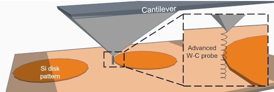
- versatile technique for nanoscale surface characterisation that enables topographic measurements with sub-nanometre resolution by means of a sharp tip mounted at the end of a flexible cantilever [1]. During operation, the tip scans across the sample surface and responds to local interactions such as van der
- the geometry of the structure, especially at the apex region, which is critical for imaging performance. Changes in tip radius, shape, or structural integrity can directly affect lateral resolution and tip–sample interaction. Therefore, although purification strategies are well established for planar


Tuning the electronic properties of defect-rich MoS2
Beilstein J. Nanotechnol. 2026, 17, 796–805, doi:10.3762/bjnano.17.56
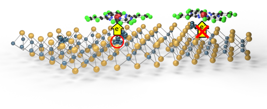
- investigated by XAS and (angle-resolved) PES using an angle-resolved time-of-flight detector (ARTOF). For XAS, the total electron yield of the sample current was measured. The energy resolution for the Co L edges was 263 meV at a photon energy of 790 eV. For photoemission at excitation energies of 900, 500
- located about 0.5 eV below EF, which corresponds to a slight p-doping (Figure 1e,f; integrated spectra: Figure 1k,l). Subsequent deposition of roughly a monolayer of CoPcF16 on the sputtered substrates causes further energetic shifts, which are small but above the energetic resolution of our experiment


Restorative potential of laser-synthesized silver nanoparticles with Salvia officinalis for periodontal disease treatment: an in vitro study
Beilstein J. Nanotechnol. 2026, 17, 781–795, doi:10.3762/bjnano.17.55
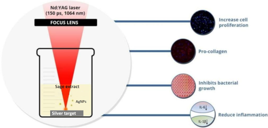
- keV with an X-FEG source and point-to-point resolution below 0.24 nm, was used to analyze nanoparticles after periods of two days and one month after synthesis. The photomicrographs were captured in the conventional mode and recorded on the CCD camera with a resolution of 4096 × 4096 pixels. The size



Substrate-dependent pore formation in molybdenum disulfide monolayers under ion irradiation
Beilstein J. Nanotechnol. 2026, 17, 769–780, doi:10.3762/bjnano.17.54
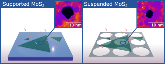
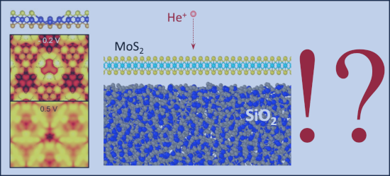
- , high-resolution scanning transmission electron microscopy (STEM) generally requires freestanding membranes, while atomic-resolution atomic force microscopy (AFM) and scanning tunneling microscopy (STM) demand exceptionally clean surfaces; also, substrate effects can further complicate interpretation
- systematically larger by ≈1 nm across all charge states. In addition, within our experimental resolution, we observe no significant dependence of pore radius on kinetic energy over the investigated range. This observation is consistent with sputtering experiments of monolayer MoS2 carried out by Skopinski et al


Tailoring Ag–Pt nanoalloys through solid-state dewetting: structural and optical insights
Beilstein J. Nanotechnol. 2026, 17, 748–759, doi:10.3762/bjnano.17.52

- presented below in Figure 10b. The obtained values showed a good agreement with the theoretical compositions, in line with the EDS measurements. To determine a detailed chemical state analysis of the elements, high-resolution spectra were also recorded. The position of Pt 4f7/2 peaks at 71.2 eV and a
- homogeneous Ag–Pt nanoalloys, high-resolution transmission electron microscopy (HR-TEM) observations were performed. Representative cross-section TEM images of two samples with various compositions are shown in Figure 8. Images for both nanostructures exhibit uniform morphology, which strongly indicates alloy
- Ntegra AFM. To obtain high-resolution, ultra-sharp probes with a tip radius <5 nm were used. Measurements were conducted in the semi-contact mode. The morphology of the manufactured nanostructures was examined using microscopic techniques. A FEI Quanta FEG 250 scanning electron microscope operating at 10




Oxidative atmosphere-driven formation of single-phase spinel CuRh2O4 nanofibers for alkaline water oxidation
Beilstein J. Nanotechnol. 2026, 17, 737–743, doi:10.3762/bjnano.17.50
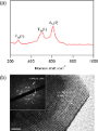
- 609.6 cm−1 (A1g), which are consistent with the spinel CuRh2O4 lattice [17][18], supporting the XRD-based phase assignment (vide supra). As shown in Figure 4b, high-resolution transmission electron microscopy (HRTEM) analysis of the electrospun CuRh2O4 nanofibers reveals clear lattice fringes with an
- characterization Morphology and elemental composition of the synthesized nanomaterials were examined using field-emission scanning electron microscopy (FE-SEM; JEOL JSM-6700F) and high-resolution transmission electron microscopy (HRTEM; JEOL JEM-2100F). Surface chemical states and crystallographic structures were




Environmental applications of silver nanoparticles: state-of-the-art review and emerging trends
Beilstein J. Nanotechnol. 2026, 17, 697–736, doi:10.3762/bjnano.17.49
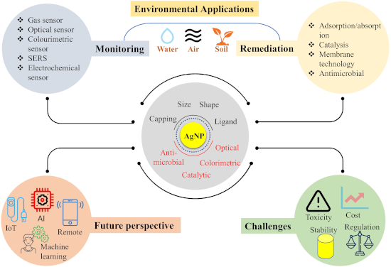
- , which calculated the AgNP concentration as particles per millilitre [53]. Microscopic techniques, such as transmission electron microscopy, provide high-resolution images of individual nanoparticles, confirming morphology, size distribution, and elemental composition when coupled with energy-dispersive


Decontamination from water pollutants and pathogens by electrospun nanofibers doped with heavy-atom-free borafluorene-BODIPY photosensitizers
Beilstein J. Nanotechnol. 2026, 17, 668–682, doi:10.3762/bjnano.17.46
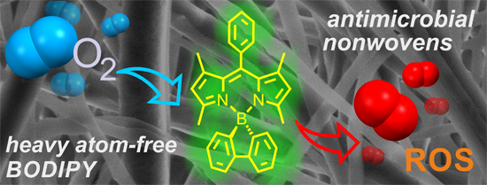
- eV (scanning step 0.05 eV) for high-resolution spectra acquisition. To compensate charging effects, the Kratos charge neutralization system was used. The binding energy scale was calibrated with respect to the C–C component of C 1s spectra (284.8 eV). The acquired spectra were analyzed using CASA XPS
- ® software and embedded algorithms. The components of the high-resolution spectra were represented with Gaussian (70%) and Lorentzian (30%) lines, while the background was represented with Shirley’s function. Water contact angle measurements and surface free energy determination The wettability of all
- nitrogen (N 1s at 400 eV), while boron was not detected due to lower sensitivity of XPS for boron. The decomposition of the C 1s high-resolution spectrum (Figure 6b) gives four components located at 284.8, 286.2, 287.2, and 288.8 eV, which can be assigned to C−C, C−O/C−N, C=O, and O−C=O, respectively



afspm: A framework for manufacturer-agnostic automation in scanning probe microscopy
Beilstein J. Nanotechnol. 2026, 17, 653–667, doi:10.3762/bjnano.17.45
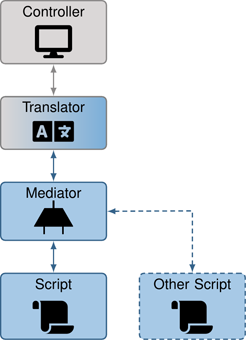
- occur whenever two suitable scripts request control. Given our assumption of a single “primary” script, this is mainly problematic if certain experiment problems are interdependent and the resolution order is important. This can be avoided by extending the mediator to accept a problem hierarchy on
- , the high volume of controls available in most SPM controllers make the task of creating a fully comprehensive framework impractical. We chose to focus on the most common actions and parameters (Table 2); these are running and configuring scans (the physical region and data resolution), running and




Two-step laser synthesis of Ag@TiO2 nanomaterials for the photocatalytic degradation of rhodamine B
Beilstein J. Nanotechnol. 2026, 17, 622–634, doi:10.3762/bjnano.17.43
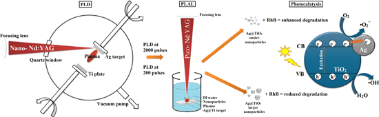
- resolution by detecting emitted secondary electrons (SE) for topography showed that there is a small difference in surface morphology between Ag@TiO2 200p and Ag@TiO2 2000p plates. This could be correlated with the silver distribution and concentration on the titanium plate. EDS analysis showed a homogeneous
- microstructural examination utilizing transmission electron microscopy. Investigations were conducted using scanning transmission electron microscopy, high-angle annular dark-field with energy-dispersive spectroscopy, and conventional and high-resolution transmission electron microscopy. A drop of the suspended


Probing tribological evolution in atomically thin MoS2 at different scales
Beilstein J. Nanotechnol. 2026, 17, 586–597, doi:10.3762/bjnano.17.40
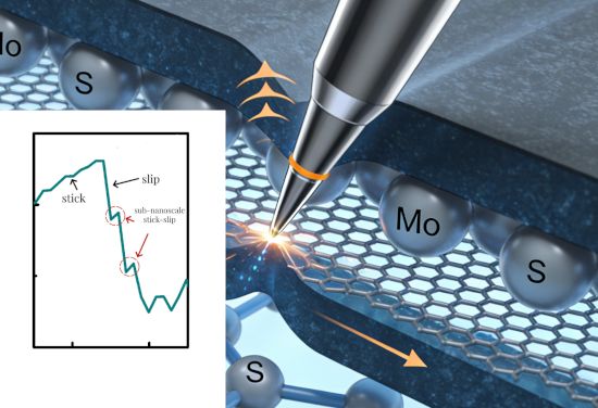
- 2D materials remain elusive, primarily due to the need for high resolution and precise control of tip–sample interactions. Atomically thin 2D materials are ideal platforms for studying nanoscale and sub-nanoscale friction, owing to their atomic smoothness, well-defined crystal structure, and chemical
- , leading to a corresponding reduction in slip distance and the quenching of sub-nanoscale stick–slip events. It is worth noting that the MFP-3D system used in this work has a maximum sampling rate of 1 MHz (time resolution of 1 μs), which is indeed much lower than the picosecond-scale sub-nanoscale stick
- –slip motion predicted by MD simulations [11][12]. This temporal resolution limitation means that our experiment cannot capture the transient dynamic process of individual sub-nanoscale stick–slip events, but only the cumulative spatial and force response of these events during the slip phase of


Impacts of annealing on structural and photophysical properties of zinc phthalocyanine adsorbed on graphene
Beilstein J. Nanotechnol. 2026, 17, 576–585, doi:10.3762/bjnano.17.39
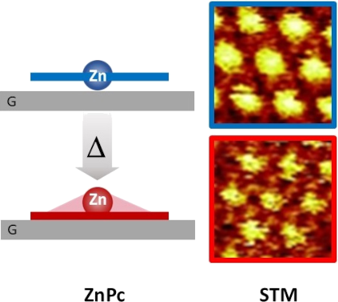
- resolution (≈1 µm) both Q-band absorption peaks are uniformly distributed all along the considered area of the sample. This holds also for the intermediate situation, showing that the spectral effect of annealing does not involve a 2D phase transformation with domains larger than the micrometer. Fluorescence
- TSB35 monolayers [46]. Given the robustness of the TSB35-C12 matrices, it is not surprising that such behaviors are preserved in the presence of trapped ZnPc. The lattice constant, 4.3 nm, is also preserved, as imposed by the TSB35-C12 matrix [39]. Secondly, and more pointedly, the high-resolution STM
- substrate) the ZnPc STM image recenters on the central Zn atom and the visibility of the TSB35-C12 conjugated cores, relative to ZnPc, is improved. Such a better resolution (i.e., a smaller spot size produced by the central Zn atom) is also characteristic of reduced fluctuations through a tighter anchoring


Laser–material interactions in liquids for the synthesis of nanomaterials: current status and perspectives
Beilstein J. Nanotechnol. 2026, 17, 571–575, doi:10.3762/bjnano.17.38
- techniques capable of probing the initial stages of nanoparticle synthesis with high temporal and/or spatial resolution [32][33]. In particular, accessing the picosecond time window needed to capture the initial interaction of the ablation plume with the liquid environment, which defines the subsequent
- longer-term cavitation bubble dynamics, remains challenging even for shadowgraphy employing ultrafast cameras [34]. Pump–probe reflectometry provides the required picosecond and even femtosecond resolution [35]. However, interpretation of the multi-stage reflectivity response is nontrivial and often
Electrochemical determination of ciprofloxacin using a MIL-101/reduced graphene oxide-modified electrode
Beilstein J. Nanotechnol. 2026, 17, 541–554, doi:10.3762/bjnano.17.35
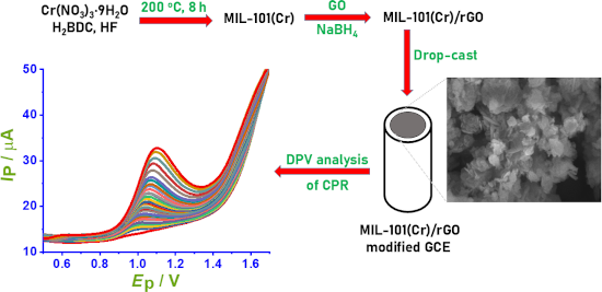
- , suggesting that the synthesized composite is predominantly composed of the expected elements within the detection limit of XPS. The high-resolution Cr 2p spectrum (Figure 3b) shows two prominent peaks at approximately 577.9 and 589.0 eV, representing the Cr 2p3/2 and Cr 2p1/2 spin–orbit components
- mapping, and (e) carbon element mapping. XPS spectra of the MIL-101/rGO (3.3): (a) survey spectrum, (b) high-resolution Cr 2p spectrum, (c) high-resolution C 1s spectrum, and (d) high-resolution O 1s spectrum. SEM observation of (a) rGO, (b) MIL-101, and (c) MIL-101(Cr)/rGO (3.3). (a) Cyclic voltammograms


Probing internal continua and atomic ultrafast charge transfer within size-controlled nanoparticles by post-collision interaction in core-hole clock spectroscopy
Beilstein J. Nanotechnol. 2026, 17, 505–514, doi:10.3762/bjnano.17.33
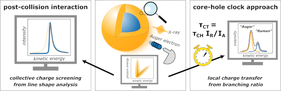
- experimental resolution (Supporting Information File 1, section 3). Therefore, the observed peak shift is primarily attributed to variations in the asymmetry of the line shape and, thus, linked to the strength of the PCI effect. The magnitude of the PCI effect, and consequently its impact on the line shape, is



Upcycling agroindustrial waste into graphene oxide supports for gold nanoparticles: toward sustainable nanomaterials
Beilstein J. Nanotechnol. 2026, 17, 489–504, doi:10.3762/bjnano.17.32
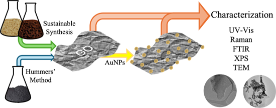
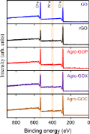
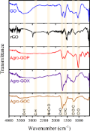
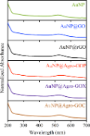
- , with an acquisition time of 30 s and two accumulations, yielding a spectral resolution of 0.8 cm−1 per pixel. Attenuated total reflectance Fourier transform infrared (ATR-FTIR) spectroscopy was performed using a Nicolet Nexus 470 FTIR spectrometer (Nicolet, Madison, WI, USA). Spectra were collected at
- room temperature in the 4000–540 cm−1 range with a spectral resolution of 4 cm−1, averaging 80 scans per sample. The surface chemical composition was assessed by X-ray photoelectron spectroscopy (XPS) using a SPECS spectrometer equipped with a PHOIBOS 100 energy analyzer and an Al Kα X-ray source (hν
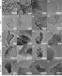
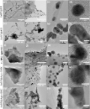
- = 1486.6 eV). The pass energy was set to 10 eV for high-resolution scans and to 40 eV for survey spectra. All binding energies were referenced to the C=C peak at 284.4 eV. Transmission electron microscopy (TEM) was carried using a JEOL JEM-2100 microscope operating at an accelerating voltage of 200 kV. TEM



Defects and defect-mediated engineering of two-dimensional materials: challenges and open questions
Beilstein J. Nanotechnol. 2026, 17, 454–488, doi:10.3762/bjnano.17.31
- scanning probe methods, can provide information on the atomic structure of materials with sub-angstrom resolution [22]. The aberration-corrected TEM has made it possible not only to obtain images of impurities [23][24][25][26] and intrinsic point defects [27][28][29][30][31], but also to follow their
- and the mechanisms of defect formation. This indicates that defects can also be created deliberately during exposure to the electron beam, which can be used for engineering structure and properties of materials with potentially atomic resolution [34][35][36][37]. It should be pointed out that many
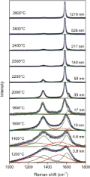
- resolution for that [113] (Figure 5c). What are the challenges in the calculations of Raman spectra of defective 2D materials? In order to correctly describe how the phonons of the pristine material are affected by defects, calculations of Raman spectra require large supercells to describe the low defect





Biomimetic nanoparticles in cancer photodynamic therapy: a review of targeted delivery systems and therapeutic outcomes
Beilstein J. Nanotechnol. 2026, 17, 396–422, doi:10.3762/bjnano.17.27


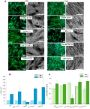
Polycatecholamine nanocoatings on stainless steel: the effect on attachment of human fibroblasts and platelets
Beilstein J. Nanotechnol. 2026, 17, 365–380, doi:10.3762/bjnano.17.25
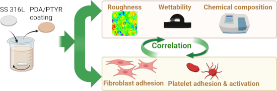
- prepared in triplicate (n = 9 measurements). The materials obtained with extreme coating times underwent for further tests, that is, PDA 10 min, PDA 24 h, PTYR 30 min, PTYR 24 h. Thickness of the coatings Microscopic imaging was performed using a Hitachi SU8230 ultrahigh-resolution field-emission scanning
- coatings’ surfaces were sputter-coated with a 10 nm layer of AuPd and visualized with an ultrahigh-resolution field-emission scanning electron microscope Hitachi SU8230 (Hitachi High-Technologies Corporation, Japan, magnification 5 000×). The imaging was done before washing and then after 1, 7, 14, and 28
- immediately after PRP separation. Samples were incubated for 90 min at 37 °C and 5% CO2. Following the incubation process, samples were washed several times with PBS to remove the unattached platelets and fixed 4% buffered paraformaldehyde. Platelet visualization was performed using an ultrahigh-resolution




Ferroelectric nanodot reservoir for neuromorphic computing
Beilstein J. Nanotechnol. 2026, 17, 352–364, doi:10.3762/bjnano.17.24
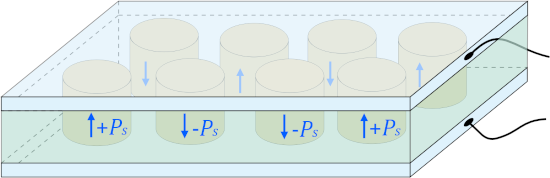
- implementations. Contactless interfaces Contactless input and output methods of data integration between the reservoir and external neuromorphic interfaces are of particular importance for the development of scalable, high-resolution, ultrafast, and non-invasive neuromorphic systems. They enable direct
- , allowing for direct control or readout of the nanodots’ polarization states with nanoscale precision. Such techniques offer a high-resolution interface with the reservoir and can be particularly effective in prototyping, diagnostics, or specialized neuromorphic functions. These contactless schemes are